After repairing my CGA video card, and building Sergey’s Micro 8088 processor board and ISA 8-bit Backplane, I am now in a position where I should be able to test the combination of cards and verify if the CGA video output is working. I should also be able to find if the Micro 8088 is behaving correctly.
Join me after the break to read about the journey. Fair warning that this post is a long one. Hopefully you will find it interesting or at the very least entertaining to observe my failures and the strategies employed to work around them.
More Things Needed
Although I have most of what I need, There are a few additional components required.
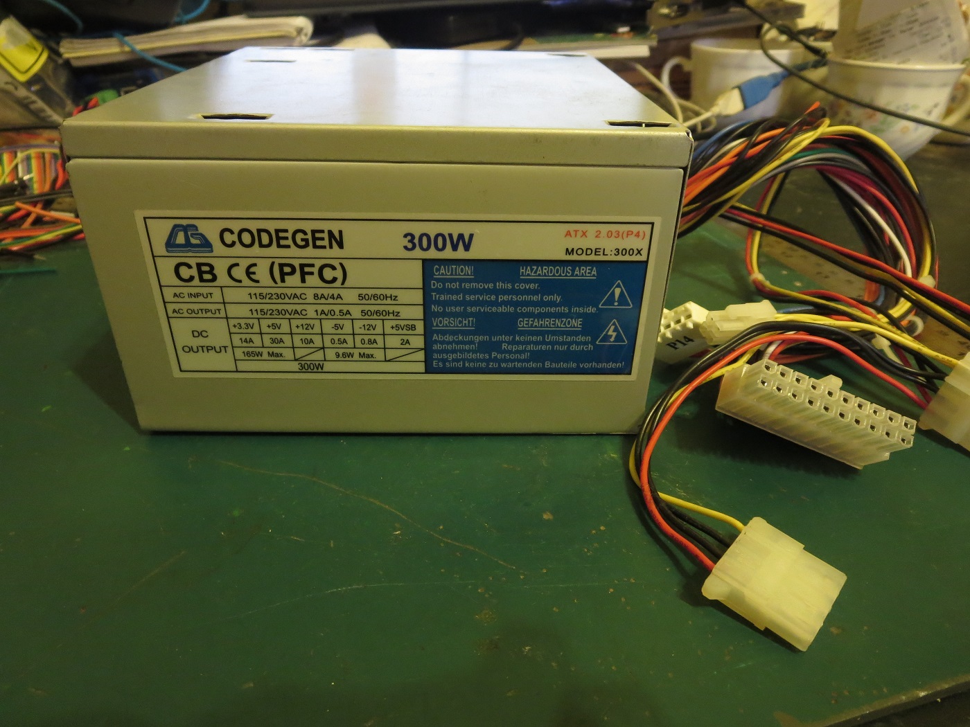
One additional component is an ATX power supply that will fit the molex connector on the ISA 8-bit backplane. Fortunately, I managed to find an old ATX power supply from the early 90’s that should work. This appears to be an older-style ATX supply with a 20-pin connector. Newer ATX supplies should work of course; the 24-pin connector would just overhang the white plastic connector on the backplane board.
Another additional component is a signal converter that will take the composite video output from the CGA card and convert it to HDMI for display on my computer monitor. I found a cheap and simple converter from a local electronics store:

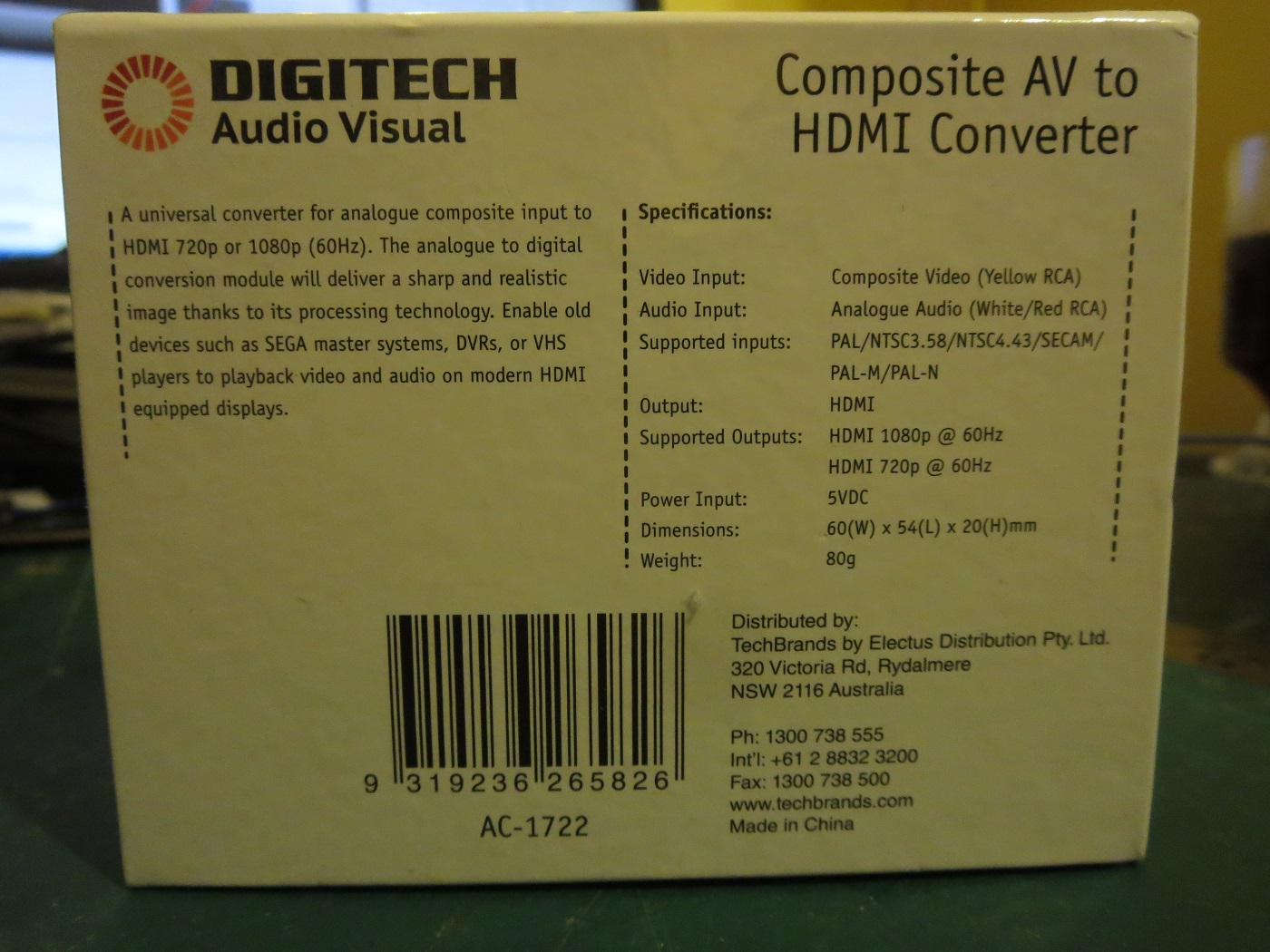
I don’t strictly need this converter, as modern TVs should take a composite signal input via a special pigtail/dongle, but I like to do my testing within reach of my regular computer. That means piping the video signal to HDMI and feeding into my computer monitor. I’m assuming this adaptor is just a re-branded one from China.
Lastly, some cables are required. One male-to-male RCA cable (to connect the CGA card to the HDMI converter) and an HDMI cable to connect to the computer monitor.
Approach to Testing
I’ll be taking a bit of a cautious approach to testing this setup. I want to:
- Verify that the backplane is working before plugging anything into it.
- Plug the Micro 8088 into the backplane on its own to verify that it is functioning to some degree of satisfaction.
- Plug in the CGA card with the Micro 8088 to attempt to get a video signal output.
Unfortunately I will be doing all of this “blind” in a sense; there is no easy way to tell at a glance what the Micro 8088 or the CGA card are doing. There are dozens of things that may go wrong that I will not immediately be able to see or diagnose. This is a frustrating experience for people new to electronics as a hobby. My advice is: always seek to measure what you cannot see with the naked eye.
I would recommend having at least a multimeter at hand, as a tool to help inspect what the circuits are doing. In my case, I will rely heavily on an oscilloscope to see the various signals on these boards.
Testing the Backplane
The first step is to plug the ATX power supply into mains power, and then plug the 20-pin molex connector into the backplane. The “Activity” LED should immediately turn green:

This is a good start; the green LED implies that the backplane is receiving standby power from the ATX power supply, as intended.
A way to verify the quality of the standby power is to measure the voltage on Pin 14 of chip U2 (the mounting holes on the board give access to the ground plane):
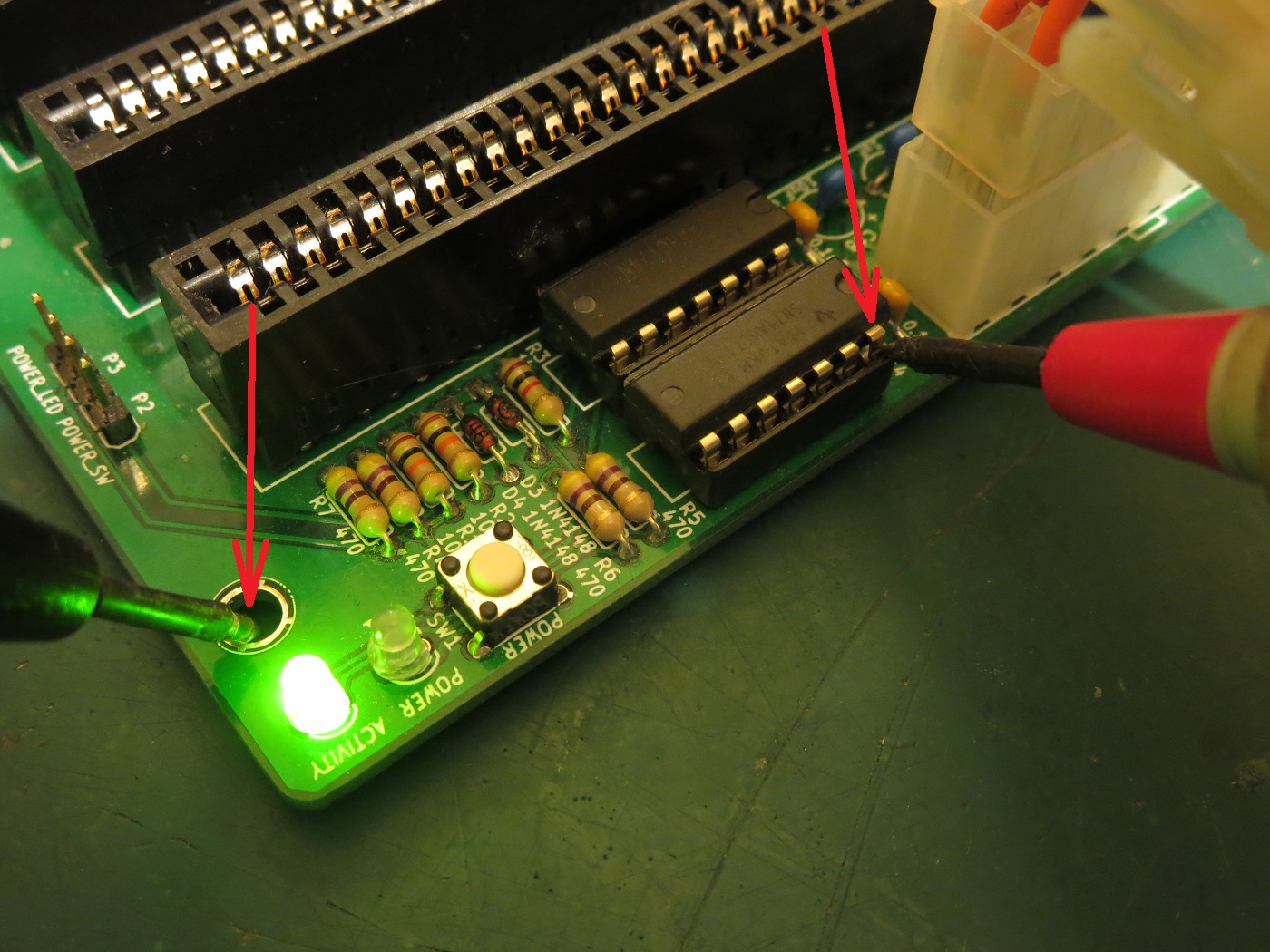
The voltmeter shows 4.940 volts of standby voltage, which is perfectly fine. Standby voltage should be close to 5 volts.
Next step is to press the power switch on the backplane. The power supply should spring to life (in my case a fan begins to run) and the “Power” LED should turn blue:
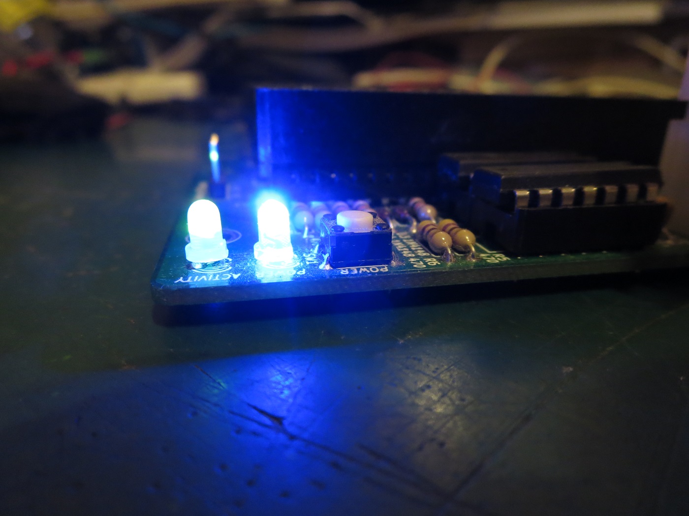
Great. This shows that the power switch on the backplane is latching into the “on” position and instructing the ATX power supply to turn on.
Now we check that all of the voltages are being generated as expected.
In order to check the +5 volt rail, we measure the voltage at the “+” side of capacitor C1 (using the adjacent mounting hole as a ground reference):
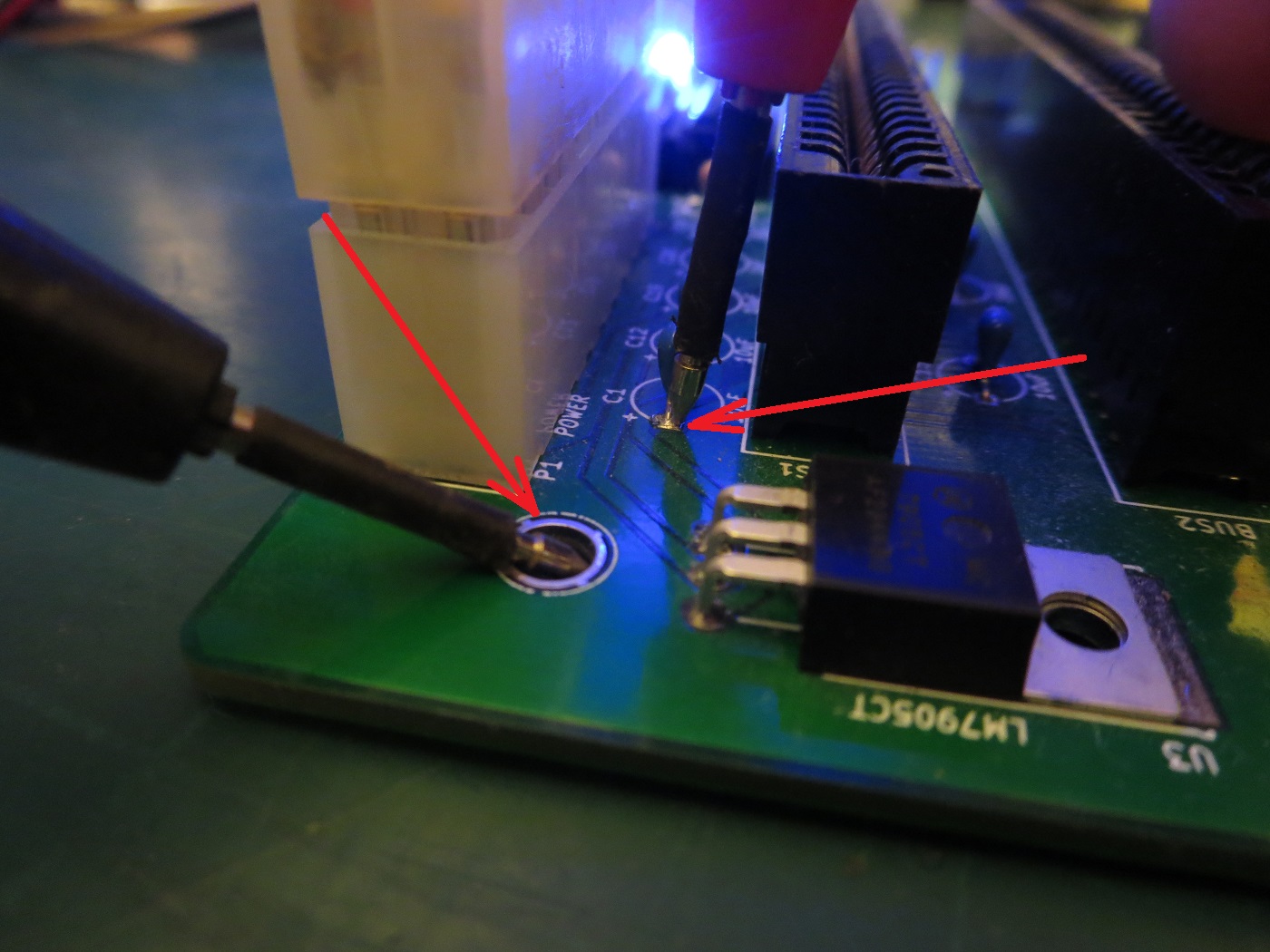
The measured voltage is 5.151 volts. This is a touch high but perfectly fine; it is likely that the ATX power supply will output a slightly higher voltage if there is no connected load.
In order to check the +12 volt rail, we measure the voltage at the “+” side of capacitor C9 (using the adjacent mounting hole as a ground reference):
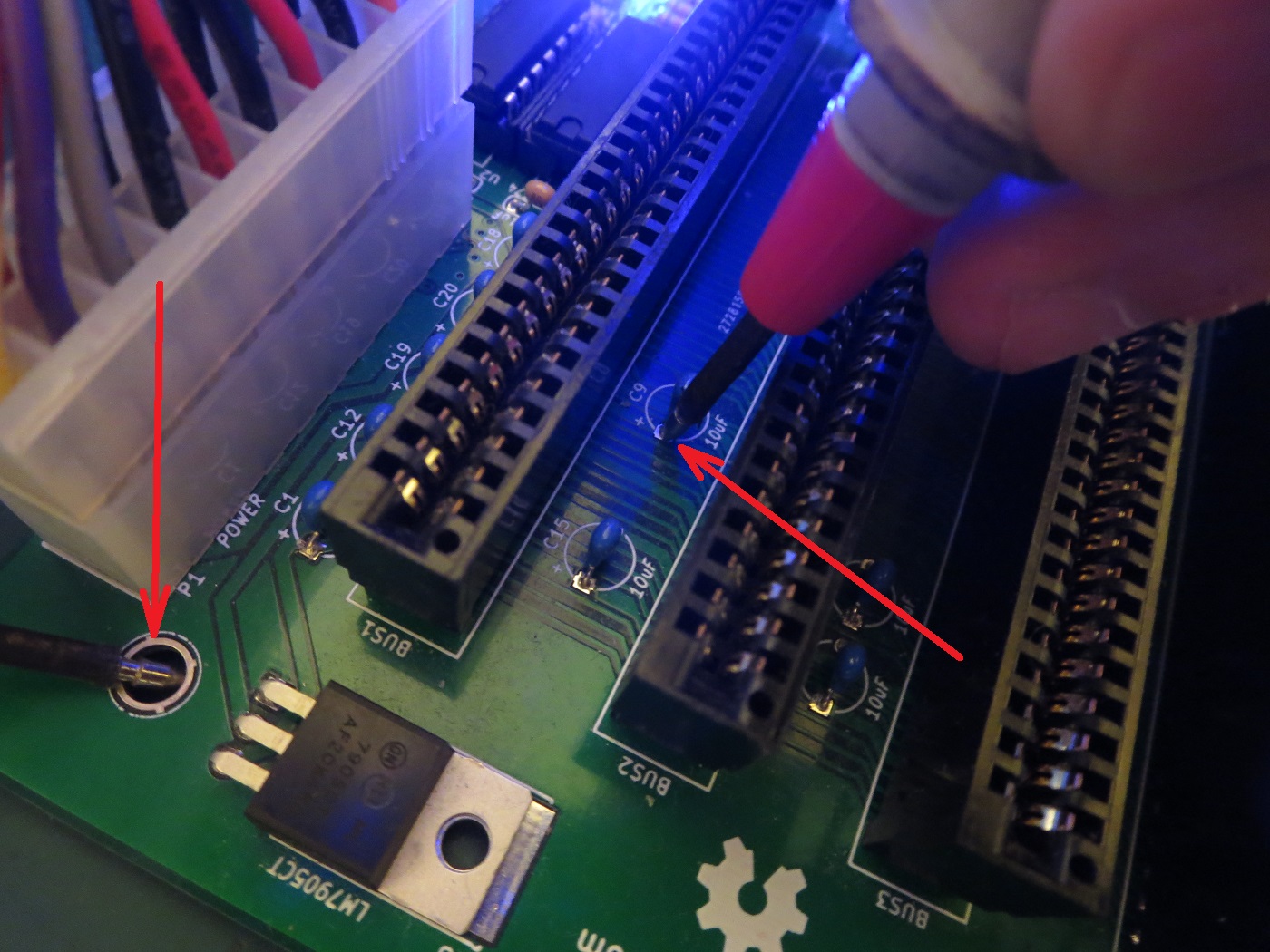
The measured voltage is 12.03 volts. This is perfectly fine.
In order to check the -5 volt rail, we measure the voltage on the pin of U3 that is closest to the edge of the board (using the adjacent mounting hole as a ground reference):
The measured voltage is -4.974 volts. This is perfectly fine.
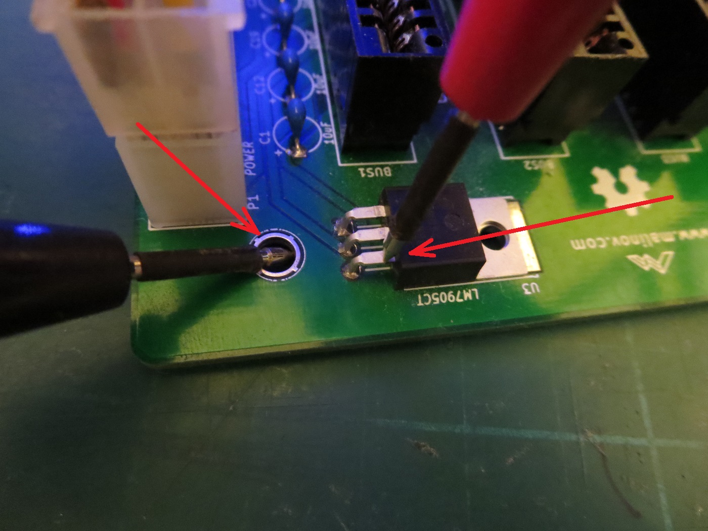
In order to check the -12 volt rail, we measure the voltage on the middle pin of U3 (using the adjacent mounting hole as a ground reference):
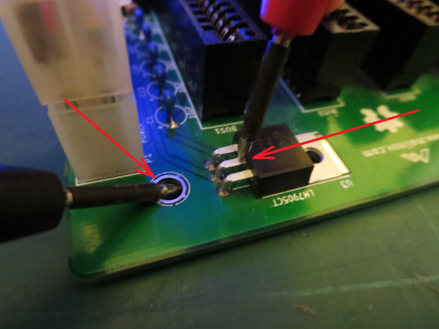
The measured voltage is -11.13 volts. This is a touch low but close enough. I’m not aware of many expansion boards that actually require the -12 volt rail.
So, nothing has blown up, and all of the required voltages are present within some tolerance. I’m comfortable enough to continue on to adding the Micro 8088 board to the backplane.
Testing the Micro 8088
Following the test of the backplane, the next step is to insert the Micro 8088 into any of the ISA slots:

After gathering all the courage required, the next step is to press the power button on the backplane. The green power LED (D2) should light up on the Micro 8088:
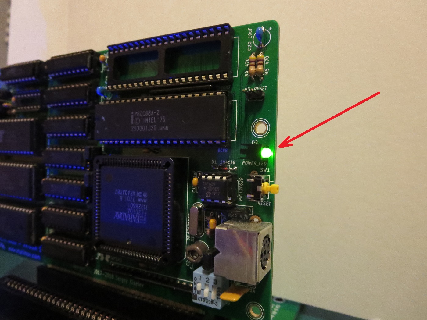
Things start to get difficult now; we have no good way to see what is happening with the Micro 8088 board. It could be executing the BIOS code as intended, or it could be broken and doing nothing.
Something we can check is the generation of the two clock signals that are distributed to the backplane and on to the other ISA slots. If the two clock signals exist, then there is a higher chance that the Micro 8088 board is functioning as intended.
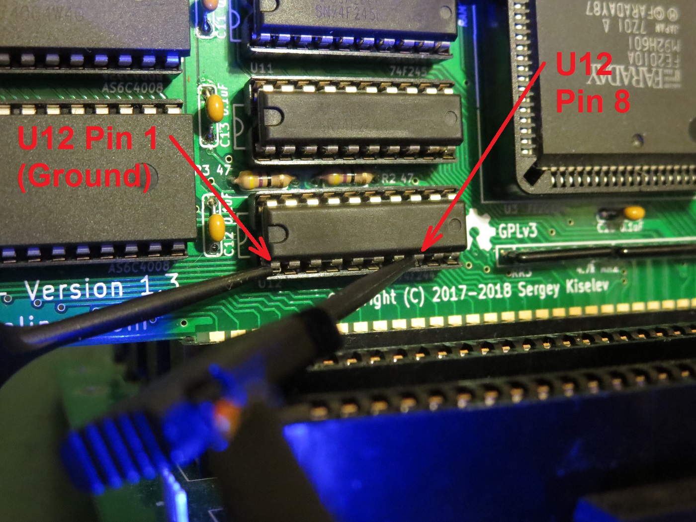
The first of the two clock signals is “OSC” which comes from pin 20 of the FE2010A. This signal is fed into pin 2 of chip U12 where it is buffered and then output through R3 onto Pad 30 of the ISA card edge connector. Using an oscilloscope, we can tap onto pin 2 of chip U12:

The oscilloscope shows:
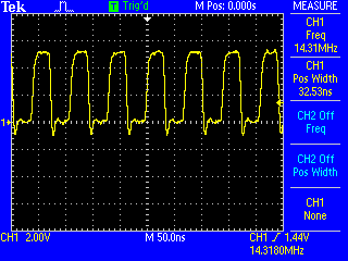
This is a good sign! The oscilloscope shows that the “OSC” signal is being produced by the FE2010A, and it is oscillating at a frequency of 14.3180 MHz. The “OSC” signal is supposed to be 14.31818 MHz. If desired, the variable capacitor C21 could be used to “dial in” the measured frequency closer to the ideal value. I will leave it as-is.
The second of the two clock signals is “CLK” which comes from pin 19 of the FE2010A. This signal is fed into pin 8 of chip U12 where it is buffered and then output through R2 onto Pad 20 of the ISA card edge connector. Using an oscilloscope, we can tap onto pin 8 of chip U12:
The oscilloscope shows:
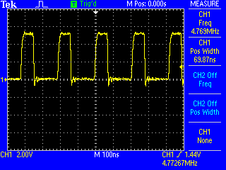
Another good sign! The oscilloscope shows that the “CLK” signal is being produced by the FE2010A, and it is oscillating at a frequency of 4.77267 MHz. In normal operation, the “CLK” signal is supposed to be 4.77 MHz. This is close enough to correct that I’ll leave it alone for now.
This is about the limits of what can be tested easily. Because both of the clocks are oscillating, I can only assume that the Micro 8088 is working correctly.
Note: There is a much easier way to verify that the Micro 8088 is executing the BIOS; by using a “POST Card“. This type of card is designed to display a series of diagnostic codes that are generated by the BIOS as it reaches certain milestones in its execution, and pushed to the card for display. I’m not using one here because I do not own one. I will certainly plan to add one to my arsenal of tools.
Testing the repaired CGA
Somewhat (minimally?) satisfied that the Micro 8088 is functioning normally, we turn our attention to the repaired CGA board. I begin by plugging it in to any available ISA slot on the backplane:

At this point in time, I also connect the HDMI converter to the composite output of the CGA card via the RCA cable, and then connect the converter to the computer monitor with an HDMI cable.
After gathering more courage, the next step is to press the power button on the backplane. Unfortunately for me, nothing happened:
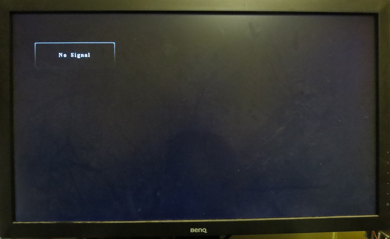
No image is displayed on the computer monitor. Very disappointing.
This is where I hit a brick wall, so to speak. The CGA ought to be working correctly at this stage, but clearly it is not. Thus begins the process of troubleshooting. In practice, it took weeks of investigating to finally break the deadlock and display an image.
Troubleshooting
For the benefit of those playing along, I’ll describe some of the steps that I took during those weeks of troubleshooting to try and diagnose the problem. This might be handy as a road-map for how to approach the troubleshooting process, especially for electronics.
Thankfully, the technical reference manual for the IBM CGA board (or at least one version of it) has been scanned and placed online. This includes a full set of schematics. We will rely heavily on the schematics to infer what the CGA should be doing.
Check the voltages
It’s very important that the voltages on the CGA card are stable. If the voltages drop below a certain level, then the chips on board may not behave as they should be. In my instance, I used the oscilloscope to check the voltages on the backplane and the CGA card (one channel for each).
In a steady-state operation no significant difference in voltage was found between the CGA and the backplane. I also repeated the test for the transient startup response, to check to see if the five volt rail was rising slower on the CGA. the rise times were more or less identical, implying that the capacitors on the CGA card have not failed and shorted the rail to ground. No obvious issues apparent here, so I moved on.
Check the clocks
There are many aspects of the CGA that are timing-critical. There are a multitude of different clocks on board, running at different frequencies, that all work together to achieve data transfer and video display. If any one of these clocks has failed, then there is a chance that the video will not display.
Clock generation on the CGA card is almost entirely controlled by U4, U5 and U6 (see schematic sheet 3 of 6) :
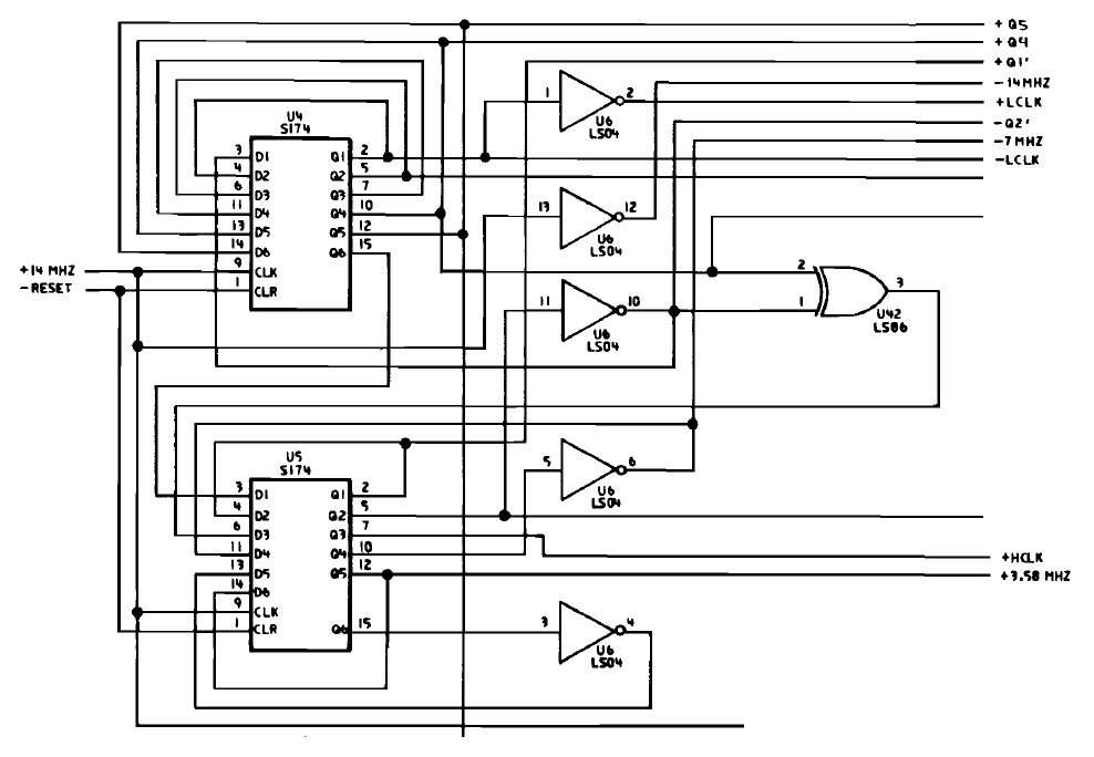
U4 acts as a “sort of” clock divider, that divides down the incoming 14 MHz clock (left hand side) to smaller specific values (see top right of schematic snapshot).
When the CGA powers on for the first time, U4 is seeded by the hex-inverter gate U6(E) which outputs onto pin 10 of U6. If this single gate is damaged, then U4 will cease to function. Checking U6 pin 10 (gate E) with the oscilloscope, no abnormalities were found.
The various clocks were measured and recorded:
| Name | Frequency |
| -RESET | 5V DC (High) |
| +14_MHz | 14.3180 MHz |
| -14_MHz | 14.3180 MHz |
| -7_MHz | 7.15899 MHz |
| +3.58_MHz | 3.57950 MHz |
| +Q1′ | 894.874 kHz |
| -Q2′ | 894.874 kHz |
| +Q4 | 894.874 kHz |
| +Q5 | 894.874 kHz |
| +LCLK | 894.874 kHz |
| -LCLK | 894.874 kHz |
| +HCLK | 1.78975 MHz |
| -HCLK | 1.78975 MHz |
All of the clocks at least appear to be running. The “+” or “-” naming convention appears to indicate the phase of the signal. There is nothing obviously wrong with the clock generation, so I move on.
Check the HD6845P
With the clocks looking vaguely plausible, the next focus of my attention is the video controller IC; the HD6845P. It appears on schematic sheet 1:

The signals of the HD6845P were measured and recorded:
| Name | Frequency |
| +VSYNC | 2.688 Hz, pulse width 2.44 mS |
| +HSYNC | 6.53193 kHz, pulse width 590 nS |
| -CCLK | 894.874 kHz |
| +DISPEN | 0 Volts DC (Low) |
| -RESET | 5 Volts DC (High) |
Which shows that the HD6845P is outputting some video timing information by way of the +VSYNC and +HSYNC signals. Another clue is that +VSYNC ought to be close to 60 Hz, instead of 2.688 Hz.
Check the Video Output Signal
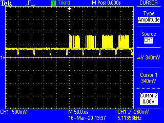
Observing that the HD6845P is working (albeit behaving a little strangely on the VSYNC frequency), it is worth while observing the composite video output signal:
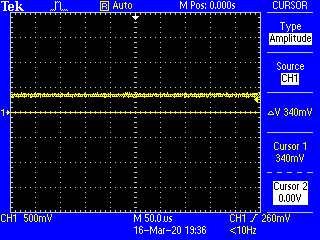
Ah-ha. There is a very rudimentary signal present on the composite output. The signal is a constant voltage, DC offset 340 mV. This is somewhat close to the NTSC IRE blanking level. The NTSC sync pulses are missing, and the video scanline data is missing.
This is telling. The basic composite signal appears to be present, but something is preventing the sync pulses and scanline data from being overlaid.
Get Lucky
As often happens in troubleshooting, I stumbled upon something critically important while browsing the schematics for the hundredth time (bottom of sheet 4 of 6):
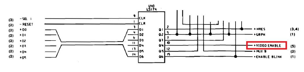
The data bus from the Micro 8088 is latched into a few different signal lines, one of which is called “+VIDEO_ENABLE”. Evidently, there is some data packet that the CGA will recognise as controlling the video output. Sure enough, the +VIDEO_ENABLE line is held low on my CGA card as the system boots.
This signal is routed to U13A, which is an AND gate located on the top right of schematic sheet 5. The output of this gate is a signal net called “-CLR_S_R”, which is routed to the Reset and Clear inputs of U35, U32, U7 and U8 located on schematic sheet 5. U32 is a data serialiser chip that outputs to a signal net called “+CHG_DOTS”. This signal (combined with other downstream circuitry) controls the overlay of line scan data on to the NTSC output waveform.
So why is +VIDEO_ENABLE not being asserted high when the system boots? This is looking more and more like a communication problem with the Micro 8088.
What of the NTSC Sync pulses?
To flesh out this investigation, many many hours were spent figuring out how the sync pulses are overlaid over the composite video output. To do this, I traced backwards from the composite video generation circuitry on schematic sheet 5 (i.e. transistor Q1 on the right hand side). It turns out the sync pulse generation is controlled by U64 and U63:

For simplicity the downstream circuitry is not shown above; all that needs to be known is that the green annotated signal nets pass to U41(C) and U42(B), from which they are combined into one net fed into U20(F). The signal is then buffered thorough U24 and fed through resistor R5 which feeds the input of Q1. Q1 drives the composite output signal from the card.
The way that U64 and U63 control the NTSC sync pulse is not immediately obvious. The exact explanation would take too long; suffice it to say that the combination of the +HSYNC and +VSYNC signals from the HD6845P (orange and purple annotations) interact with the +LCLK signal (red annotation) to form the pulse via selective annulment of the various overlapping signal levels. The signal from U64 to U63 (blue annotation) contributes to signal division between the two chips, and eventually MUX-ing of the horizontal and vertical sync pulses into the one NTSC sync pulse-train output.
From what I can see, the signals produced by the HD6845P are incorrectly timed, such that no sync pulses are generated from the U64 and U63 chip pair.
That is to say: the +VSYNC signal frequency of 2.688 Hz (pulse width 2.44 mS) and +HSYNC signal frequency of 6.53193 kHz (pulse width 590 nS) are not interacting/overlapping in such a way that produces a valid NTSC sync signal.
Digging deeper into the HD6845P datasheet, the +VSYNC and +HSYNC frequencies are configurable by writing to data registers within the HD6845P. Presumably, the Micro 8088 should be writing data to these registers to set the correct vertical and horizontal sync settings.
So perhaps some of the chip initialisation is not being performed when the system boots? This is looking even more like a communication problem with the Micro 8088.
The Eureka Moment
Dwelling on the +VIDEO_ENABLE signal and the apparent lack of initialisation of the HD6845P, the cause seemed more and more likely to be related to poor communication between the Micro 8088 and the CGA. Again I spent hours thinking of a solution. Could the data bus be out of spec? Is some other part of the CGA card broken, causing the card to miss the signals presented to it?
Again, as happens with troubleshooting, I accidentally stumbled upon a solution at random. This was the “Eureka” moment: I tried a “warm reset” of the Micro 8088.
Up to this point, I had been power-cycling the Micro 8088 and the CGA card by toggling the backplane power switch. This time, I had left the machine on for a minute or so before hitting the yellow reset switch on the Micro 8088 itself.
The oscilloscope showed activity on the composite output of the card:
And the display sprung to life:
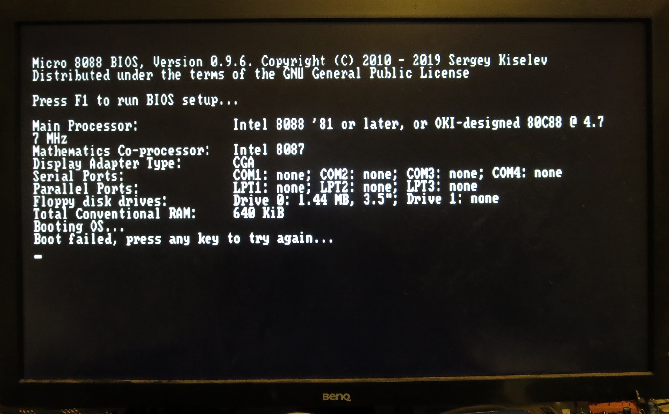
Finally!
This confirms our suspicion that there is a problem with the initialisation of the CGA card when it first powers on from a “cold” restart. I have no solid idea as to why this is occurring. It could be that:
- Sergey’s BIOS may not be waiting long enough for the CGA card to settle on first power-up before initialisation commands are issued, and subsequently they are ignored by the card.
- There may be some transient electrical behaviour in the CGA card that prevents it from accepting commands before the transients have settled. I.e. the CGA card may be taking too long to settle before commands are issued to it.
It appears that the video output will only turn on if the warm-reset occurs after the BIOS has completed the RAM check. This is why this solution never bore fruit beforehand; I was not waiting long enough before conducting the warm-reset.
The sequence of events is therefore:
- Press the power switch on the backplane board, applying system power.
- Wait ~30 seconds.
- Press the yellow reset switch on the Micro 8088.
Conclusion
Notwithstanding this awkward boot behaviour, this test shows that:
- The Micro 8088 is working correctly; the BIOS is running, and it is able to detect the CPU and co-processor chip. The RAM check passes, showing 640KiB of usable RAM. The operating system boot process predictably fails, as we have no hard disk or floppy drive presently installed.
- The repaired CGA card is outputting a valid composite video signal for the HDMI converter to use (no image would be displaying otherwise). The character ROM on the CGA card is intact (garbled or unreadable characters would be displaying otherwise). The 80×25 character mode is working (the image may not be be displaying otherwise). The video RAM is working (garbled characters or colours would be displaying otherwise).
Although I’m confused as to why the card works after a warm-reset, I will take the small victory. The next step in building a functioning machine with the CGA card will be to boot into an operating system of some kind.
Hopefully you have found this part of the journey interesting or entertaining. I’ll be sure to post any further progress with the build as it develops.