In my last retrocomputing post, I tackled the problem of Repairing my CGA video card following quite a bit of foolish childhood damage.
In this post, I’ll document the fabrication of Sergey’s Micro 8088 processor board and ISA 8-bit Backplane. The hope is that I can get my CGA video card working with Sergey’s two boards, and combine them into a functional retrocompter.
Even though I wouldn’t call myself one, I will be approaching this as though I am a complete novice. The information here is a summary of many days of trial and error, so I wish to present it for the benefit of those that may be just starting with retrocomputing as a hobby.
Fortunately, both of Sergey’s boards were gifted to me by a friend. There would be a bit of effort required to source these boards myself. As an example, the process of ordering the Micro 8088 would be:
- Navigate with a web browser to the root directory https://github.com/skiselev/micro_8088
- Click the green drop-down button “Clone or download” to the upper right of the file listing.
- Select the “Download ZIP” option from the menu.
- Choose a place to save the ZIP file on your machine.
- Unpack the ZIP file and navigate to the gerber folder “micro_8088-master.zip\micro_8088-master\gerber”
- Select all the gerber files in this folder and re-ZIP them. Call the new ZIP file something memorable. There should be the following files in the new ZIP: .drl, .gbs, .gbo, .gbl, .gm1, .gts, .gto, and .gtl.
- Visit a PCB fabrication website (PCB Zone, Seeed Studio, PCBWay, JLCPCB, etc) and follow the prompts to upload the new ZIP file that you have created.
- Choose the various board fabrication settings that achieve the desired result. You could choose custom colours, board finishes, etc as desired. See EEVblog #1259 for an excellent video explanation of these different settings.
- Confirm the order and wait several weeks for fabrication and shipping.
The same process would apply to the ISA 8-bit Backplane (and it might make sense to order both at the same time to cut down on shipping).
You could also use the KiCad project files downloaded from the Github repository ZIP file and produce the Gerber files yourself, but I’m assuming that I’ve not learned how to use KiCad just yet so I’ll skip right over that for now.
My boards arrived in the mail from my friend:

Once you have ordered the boards, you must order the components to solder into those boards.
Ordering Components
Thankfully, Sergey has done an excellent job consolidating each component list into a convenient format on Mouser (other distributors would of course carry the same sorts of components):
These lists are a great head start, but I found that some products had drifted out of production since the lists were put together by Sergey.
Errata for the Micro 8088 list on Mouser (as at October 23, 2019):
- The 10k resistors from Xicon (291-10K-RC) were on back-order. Instead I used Yageo MFR-25FRF52-10K as a substitute, but pick whatever you please. Many different equivalent brands would exist.
- The Purple-coloured Circular DIN Connector KMDGX-6S-BS2715C was non-stocked. Instead, I used 5749180-1 which is an equivalent part from TE Connectivity but coloured black. The Kycon part KMDGX-6S-BS would also probably work but I believe it also comes coloured black.
- The Trimmer/Variable Capacitor (6.5-30pF) GKG30015 was not available. Instead, I used GKG60015 which is the same general type of capacitor but with a higher range of 12-60pF. Hopefully the higher range does not pose issues.
- The 8088 CPU IP80C88-2 was not available. There is an equivalent part produced under product code CP80C88-2Z which is still available, albeit for a reduced temperature range of 0 degrees C to 70 degrees C. The cost of the CP80C88-2Z is approximately $54 AUD which was too much for my tastes. Instead, I opted to buy a second-hand 8088 cpu from Utsource (see further below).
- The 47 Ohm resistors from Xicon (291-47-RC) were on back-order. Instead I used Yageo MFR-25FRF52-47R as a substitute, but pick whatever you please. Many different equivalent brands would exist.
Errata for the ISA 8-bit Backplane list on Mouser (as at October 23, 2019):
- The -5V Linear Voltage Regulator LM7905CT was not available. Instead, I used MC7905CTG from OnSemi. Many different other options would exist as a substitute for this part.
- The blue LED SSL-LX3054USBD was in stock, but on returning to write this article, had gone out of stock. TLHB44K2M1 from Vishay should work as a substitute.
- The 10k resistors from Xicon (291-10K-RC) were on back-order. Instead I used Yageo MFR-25FRF52-10K as a substitute, but pick whatever you please. Many different equivalent brands would exist.
- The 25V 10uF X5R 20% capacitors (FG28X5R1E106MRT06) were on back-order. Instead I used FG26X7R1E106KRT06 which are 25V 10uF X7R 10% capacitors. Different rating, but should work fine.
In addition to the parts on Sergey’s lists, it is necessary to procure a Faraday FE2010/FE2010A chip. This chip very conveniently replaces the functions of a dozen-or-so other chips (Timers, Interrupts, etc) that would have been present in the original IBM PC/XT design. Unfortunately, the Faraday chip is no longer commercially available, so it must be sourced from a third party.
I ended up procuring my Faraday FE2010A from a website called Utsource. This site acts as an aggregator for many different third-party re-sellers in China. The code I used to search was “FE2010A / M92H601“. The link provided here is the listing that I used, but be aware that the link might break randomly in the future. This Faraday chip can also sometimes be sourced from Ebay.
As mentioned above, I was also in need of an 8088 CPU chip because I didn’t want to pay for a brand new one and I figured I could risk the third-party re-seller market. In the end I ordered from Utsource, searching on the code “P80C88A-2“. Again, the link provided here is the listing that I used, but be aware that the link might break randomly in the future. There would be many, many other places to source this chip. Ebay might be one.
And while we’re buying stuff from Utsource, I decided to get an 8087 FPU chip. This co-processor chip can greatly speed mathematical calculations by offloading them from the CPU. I searched Utsource for the code “D8087-1“. Again, the link provided here is the listing that I used, but be aware that the link might break randomly in the future.
I’ve found that the pinball repair market is an unexpected place to source esoteric vintage microchips. For example, Twisty Wrist Arcade currently sells a D8088 cpu for only a few dollars. They also sell many flavours of old RAM. Unfortunately for me, this place is based in the US and does not sell or ship internationally.
I’ve also found that the Electronic Goldmine can sometimes be a source of old and esoteric chips. See their “Semiconductor” category. For example, they sell MB8118-15 DRAM chips which are getting quite hard to find.
But I digress.
Assembling the Boards
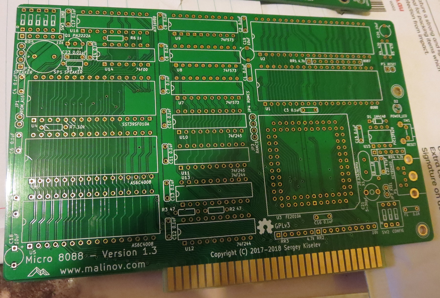
After all the parts arrived, I set about soldering them together. I didn’t get many photos of the process, but here are the final results. Note that I had not yet fitted the D8087-1 co-processor for the photo:
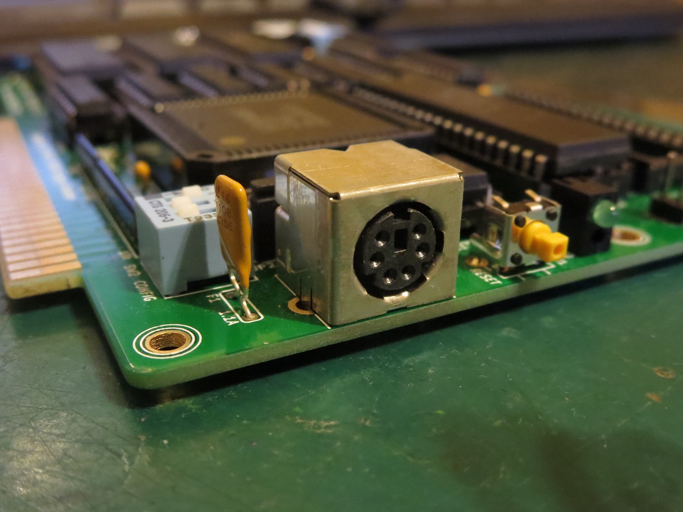
 Here’s a photo of the substituted MiniDIN keyboard connector. Note that the preference would have been to get the part with the purple plastic insert so that it’s obvious that this is a keyboard connector. But alas:
Here’s a photo of the FE2010A chip. This is actually “upside down” on the CPU board. Pay very close attention to the keying of the chip orientation as it may be easy to fit this to the socket the wrong way around. Once you’ve fitted it to the socket, you will need a special tool to remove it:

Here’s a photo of the ratty-looking P80C88A-2 CPU. When these chips come from third parties it is quite common for them to have superficial damage (scratches, dings etc). Hope it still works!:

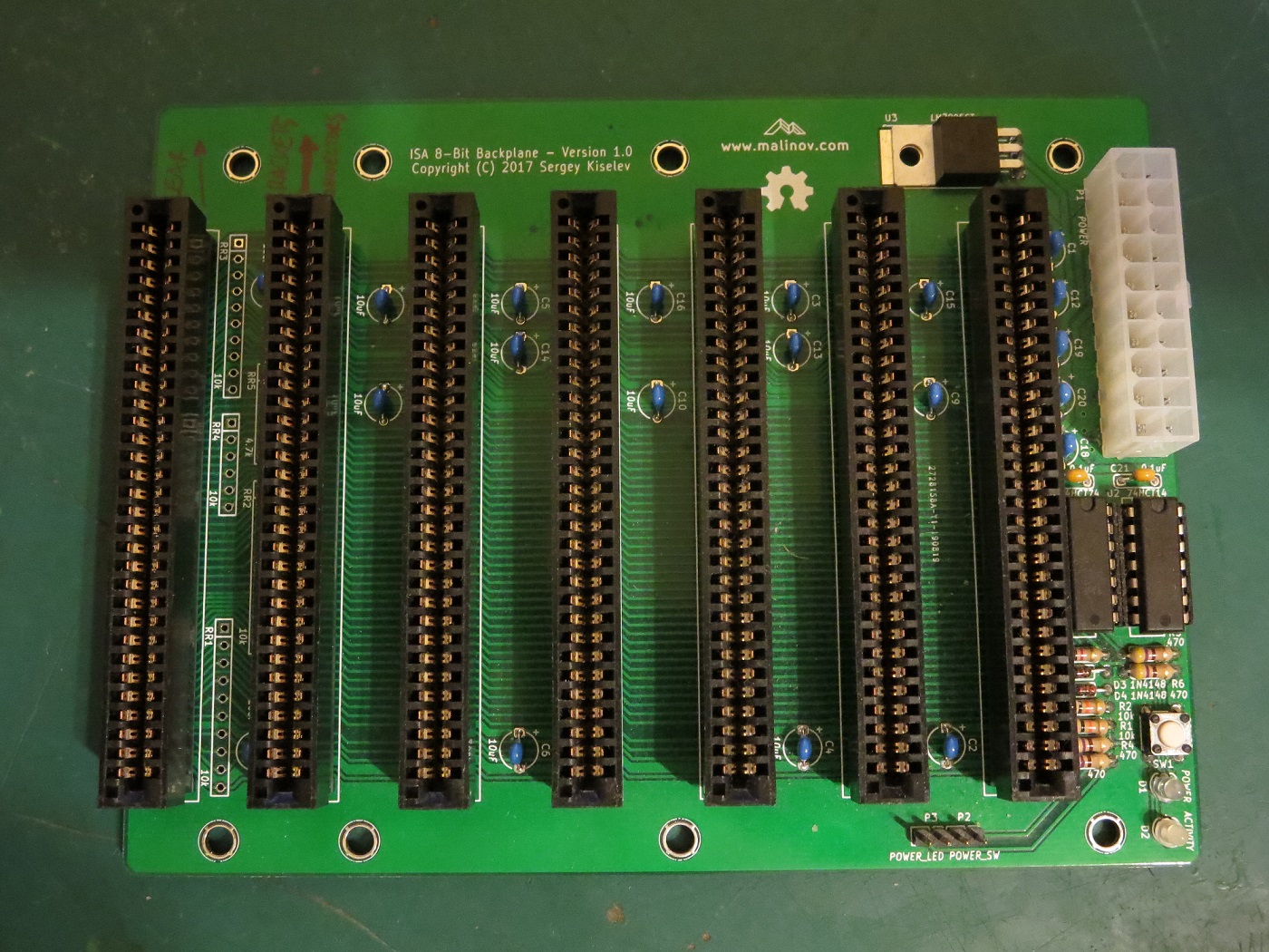
And finally a photo of the much-less-complicated backplane. Note: the proper orientation of cards in the backplane is not immediately obvious. As it turns out, the expansion card brackets should be facing the top edge of the backplane in this photo. There should be very little gap between the silver card mounting bracket and this top edge of the PCB. The keyboard connector on the Micro 8088 should face this top edge of the PCB (i.e. towards the OSH logo). Note I’ve drawn some arrows in permanent marker in the top left corner of this PCB as a reminder to myself. To really hammer this home; the expansion cards will occupy the slots and run downwards and/or overhang towards the bottom of the photo. The primary “component side” of the expansion boards will be on the right hand side of each socket when compared against the photo. The silver expansion bracket will be offset to the right of each socket when compared against the photo:
Some tips for assembling these boards:
- You might not want to load U4, U16 or U15 until after they have been programmed. They will need to be removed from the board to be programmed.
- Load the axial resistors first. Some of them are hiding between DIP sockets and may be difficult to access later.
- Load any diodes next (but not the LEDs).
- Check the height of the capacitors and the resistor arrays against the height of the DIP sockets. If the DIP sockets are taller, then load the capacitors and resistor arrays first. If the DIP sockets are shorter, then load the DIP sockets before the capacitors or resistor arrays.
- When loading the DIP sockets, place the PCB on a flat surface and load each DIP socket loose in place (without soldering). The legs will rest in the through-holes. Lift the edges of the board carefully so that the DIP sockets “drop” in place against the PCB. Hold the PCB horizontal by its edges with one hand, and with the other, place a rigid flat item over the sockets on the top side (hardcover book or a piece of glass, etc). Once the rigid flat item is in place, press the PCB upwards against it, and then flip it and the item over 180 degrees. You should be left with the sockets resting upside down, with the PCB resting on top of them, with all DIP socket legs accessible for soldering. This is why it’s worthwhile checking the height of the capacitors and resistor arrays, otherwise the DIP sockets would be spaced off of the board.
- Do not load the PLCC socket or keyboard connector until you have loaded the crystal and associated components.
- Don’t linger too long soldering the trimmer-capacitor in place; the body of this cap is made with very soft plastic.
- Put the caps in the backplane before the black rectangular connectors; it will be easier to stage it that way than feed the cap legs between the connectors.
- The black rectangular connectors can be loaded into the backplane very last. They protrude above all other components.
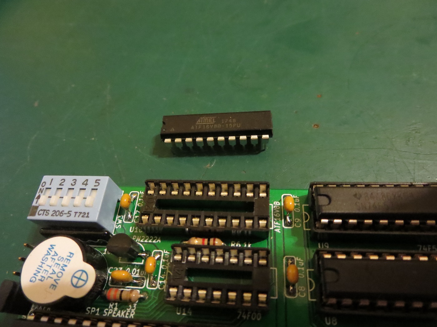
- On the Micro 8088 board, you must choose between loading in U14 (74F00) or U16 (ATF16V8B). Do not load both. The difference between them is: U14 is a simpler chip and causes some memory functions to be handled by the FE2010 in a somewhat limited capacity. U16 grants access to greater amounts of memory and offloads the function from the FE2010. The downside to U16 is: it is a special type of chip (SPLD) that must be programmed with special code in order to function. If you don’t have any way to program U16, then avoid loading it for now. I’ll cover the programming of U16 below.
Programming Chips
Are we done yet? No. We must now program some chips in order to get the CPU card functioning. For me, this was probably the most time consuming and annoying part of the whole exercise.
Notably, we must:
- Load the BIOS into the flash chip U4.
- Load the keyboard conversion code into U15, which is a PIC12F629.
- Program U16 (because in my case I chose to load U16 onto the board and not U14).
The IC Programmer
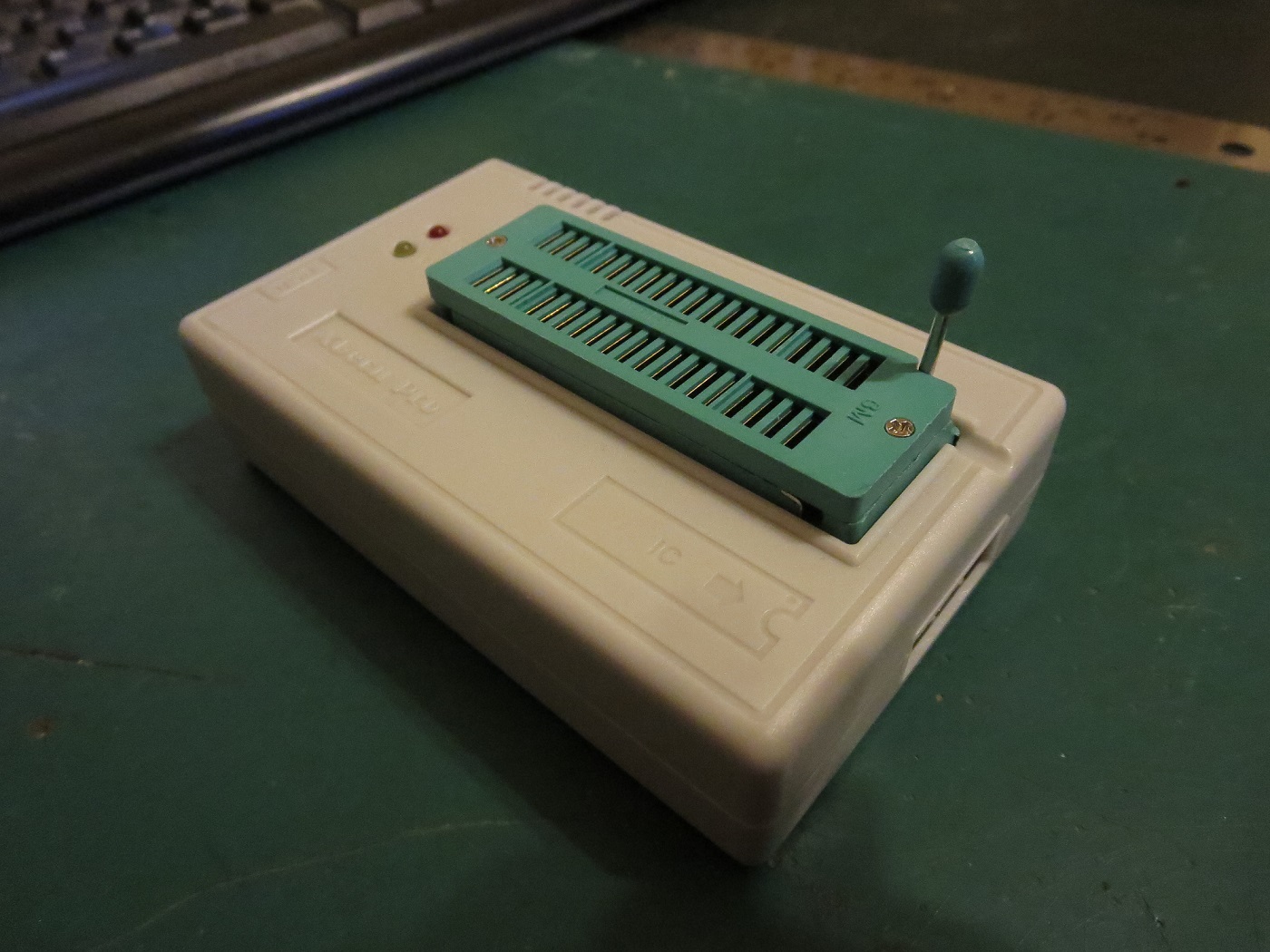
Where to begin? Ultimately, I decided to purchase a universal IC programmer from Ebay, as it was looking to be the cheapest option compared to many separate professional programming systems.
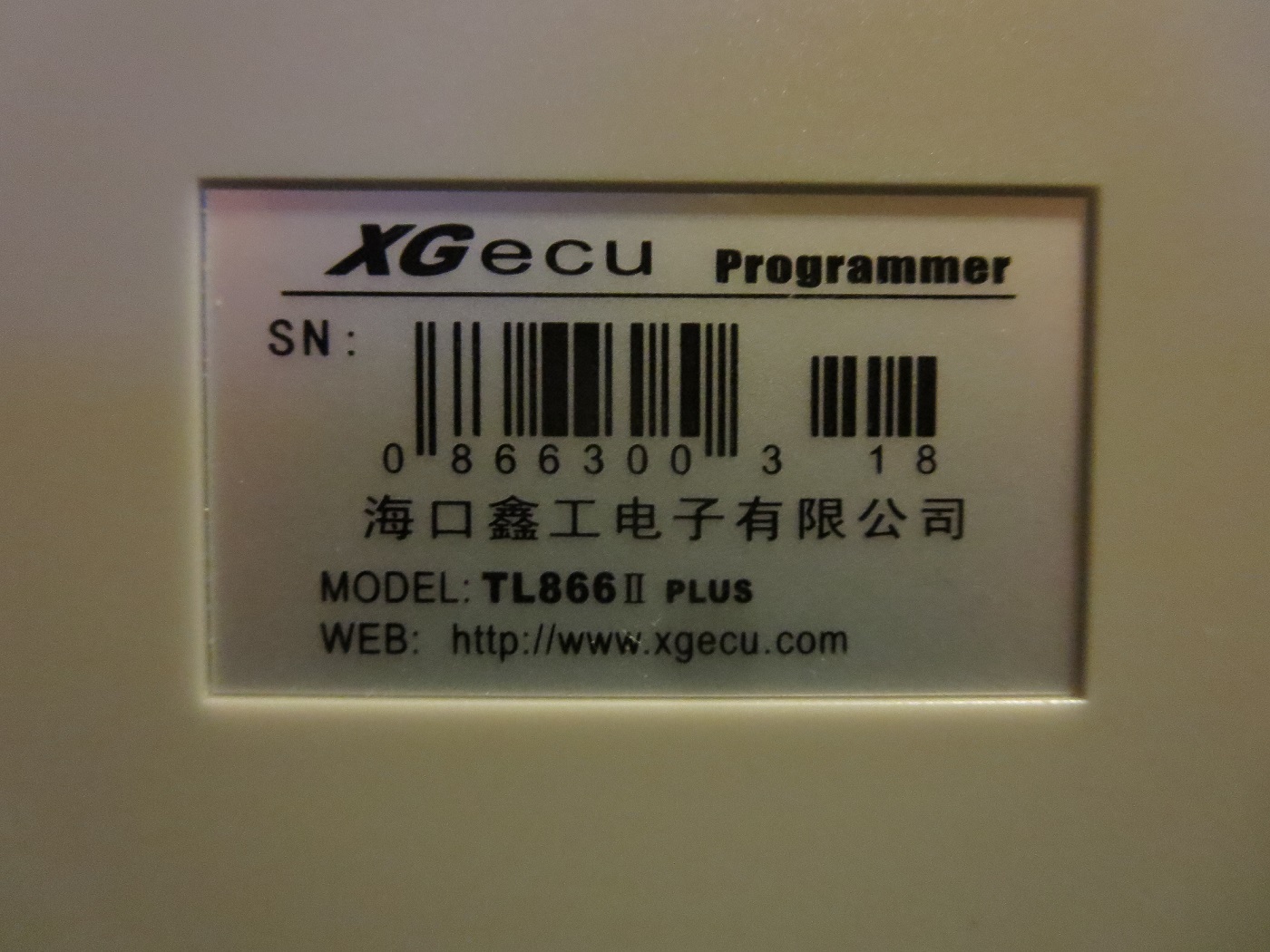
The programmer I bought was from a seller called xgecupro. The programmer was bought with a bundle of other chip adaptors and cables etc. The programmer itself was Model “TL866II PLUS”. You shouldn’t need to buy any chip adaptors in this instance as we are only dealing with DIP packages, but get whatever is cost effective to you if you are buying one.
I bought the programmer and accessories in an Ebay listing titled “XGecu Programmer TL866II PLUS for SPI Flash NAND EPROM MCU PIC AVR GAL+7 adapter” again from the seller called xgecupro.
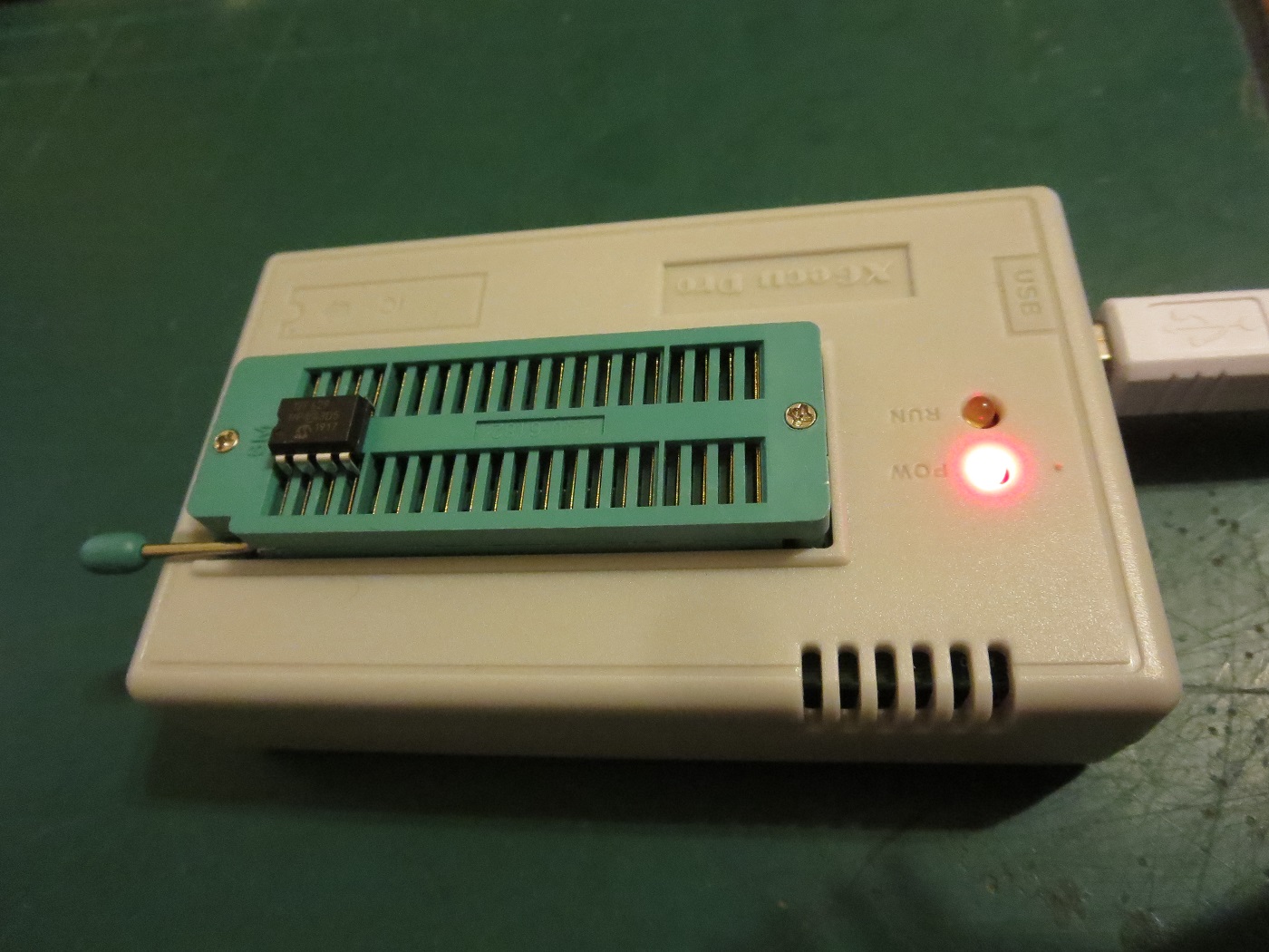
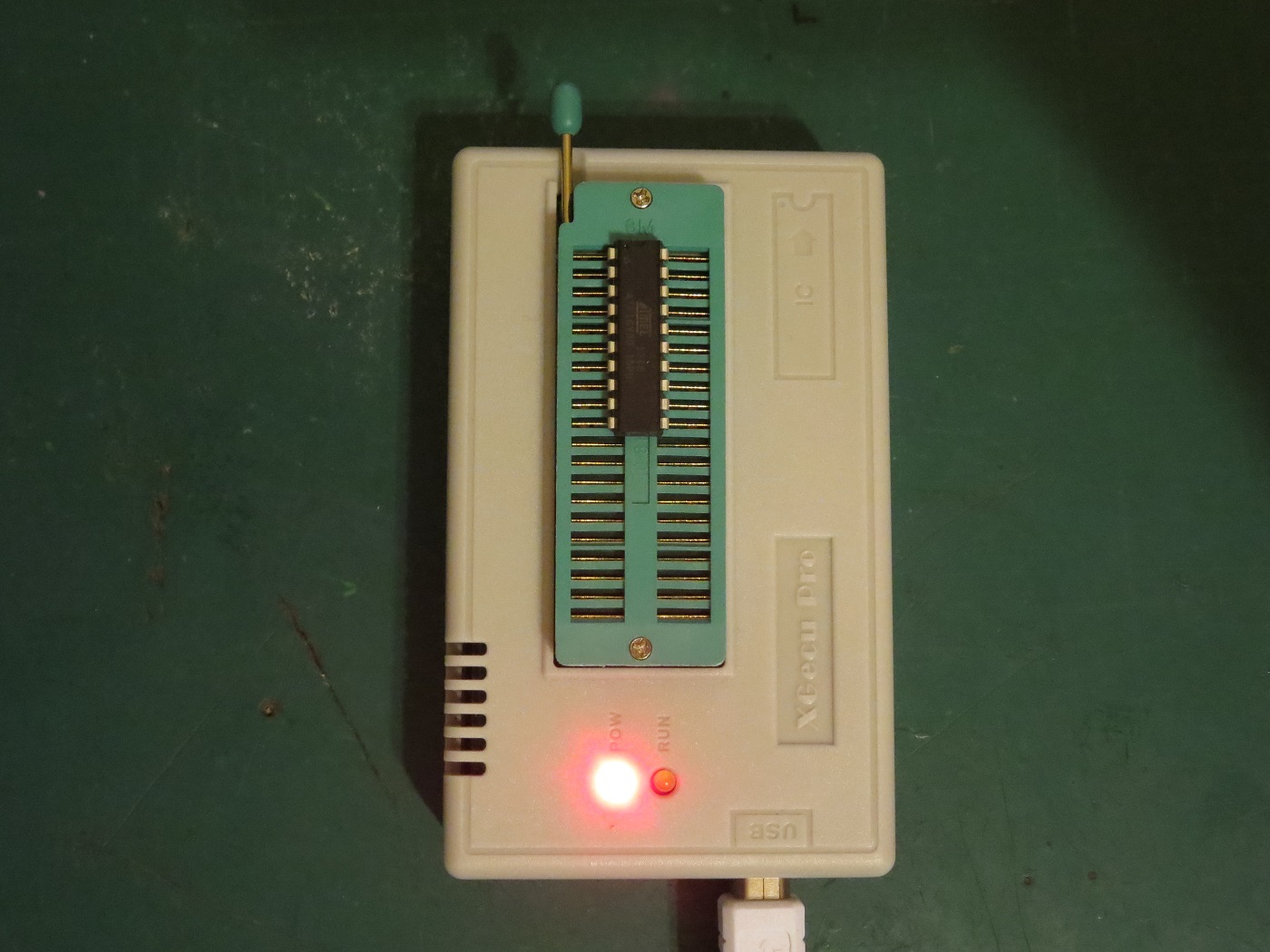
When the programmer arrived, this is what it looked like:

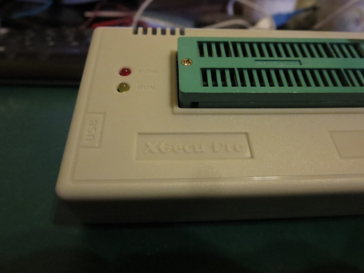
I have absolutely no idea if XGecu is the “official” supplier of this programmer, or if this is a knockoff. Let’s hope it works.
Next step. Software for the programmer. This is where I wasted most of my time. I had inadvertently bought the programmer without an installation CD. The documentation helpfully points me to the XGecu download site which is a Chinese site hosted on a Chinese domain. The site itself will load. The download link is adjacent to the title “TL866II Plus Programmer Application Software V8.51 (Chinese/English)”. But the actual download link, when clicked, timed-out every single time I tried to download the software. I guess the Chinese firewall was having a normal one. I had no success downloading the software during the dozen-or-so times that I tried.
[2020/09/03 Editor’s note: The V9.16 version of the software can be downloaded from the XGecu website as of today, from this download link. Not sure how long that will last].
Frustrated by that failure, I learned that someone had created an open-source software to communicate to the programmer. See https://gitlab.com/DavidGriffith/minipro/. Unfortunately for me, this software is primarily meant to target the Linux OS. The closest thing I have is a Raspberry Pi 3 running Raspbian. I’m not used to how that all works, but I tried anyway on the Raspberry Pi. I could check out the repo, do the install, but when it came to actually using the software it just did not want to work correctly (couldn’t read the contents of chips, would just hang randomly, etc). I gave up.
Frustrated by that failure, I scoured the Internet for any copies of the “official” software that might be hosted outside of China. I did manage to get one hit; a forum called “Lab-One” hosting a thread on TL866II Plus & TL866 Programmer Software. The software was included as an attachment to the forum post.
I don’t really trust this software that I have found, but it’s the best option I have to get things working. I installed it on an old laptop that I rarely use. No antivirus warnings were triggered on Windows 7, but 4 out of 51 scanning engines on Virustotal flagged suspicious activity. Not very happy about that, but we press on.
[2020/09/03 Editor’s note: The V9.16 version of the software downloaded directly from XGecu is flagged by 1 out of 61 scanning engines on Virustotal].
Flashing the BIOS
Probably the most important chip to program is the BIOS. This is the collection of code that will run when the computer first boots, and enables the loading of an operating system.
Thankfully, Sergey has provided a functioning BIOS for the Micro 8088 CPU board. To me, an astonishing achievement. Thank you Sergey for providing this open source to the community.
Copies of BIOS images are held in Sergey’s Github page for the Micro 8088: https://github.com/skiselev/micro_8088/tree/master/BIOS. They would also have been copied across into the ZIP file of the Github repository, if you followed that step at the start of this post in order to extract gerber files.
There are two copies of the latest BIOS:
- bios-0.9.6-xtide.bin
- bios-0.9.6.bin
I believe that the “xtide” version of the BIOS image contains the code necessary to run an IDE adapter card without a BIOS expansion ROM. For now, I’ll just focus on the non-xtide version.
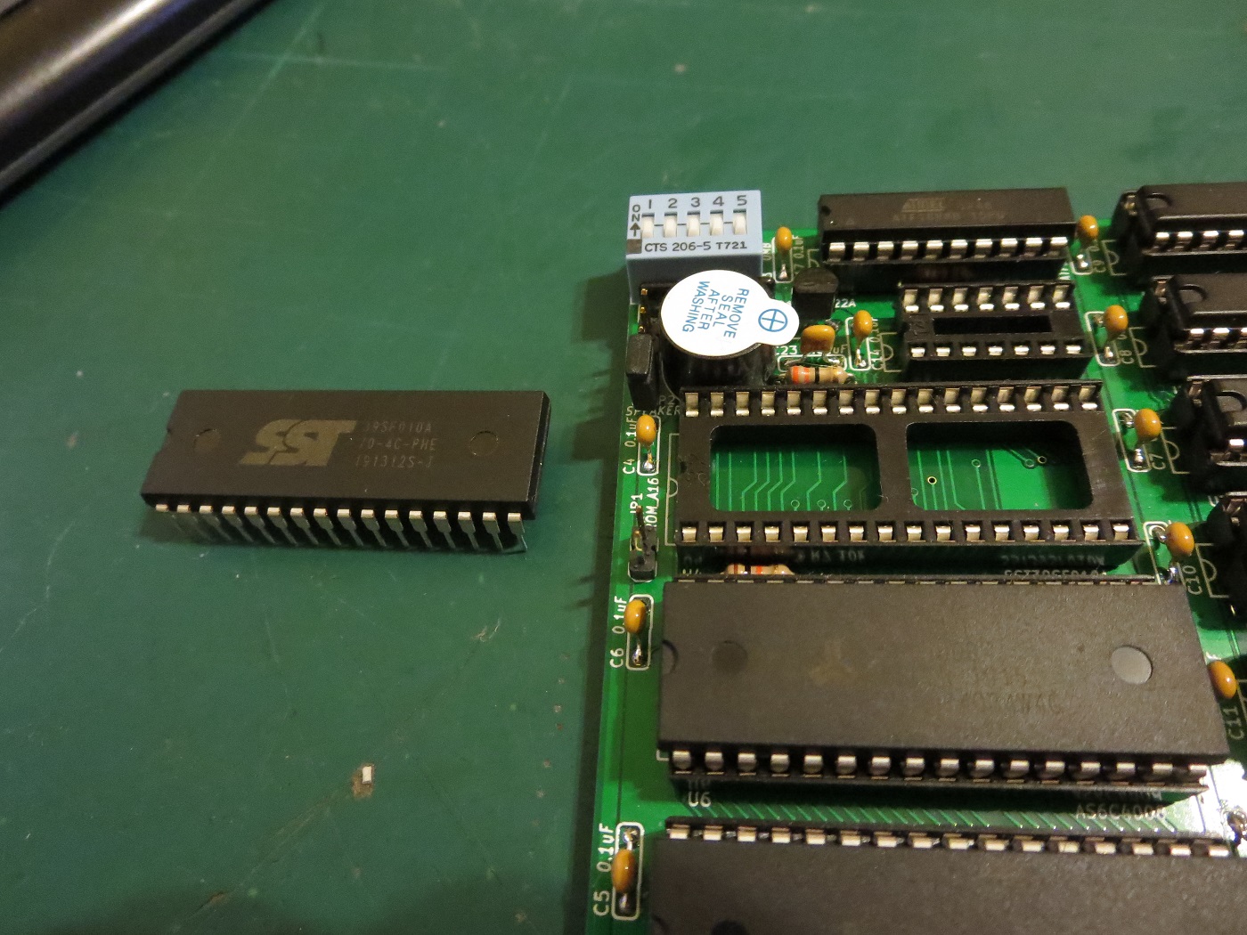
If you loaded the flash chip U4 (SST39SF010A) into its socket like I did, start by removing it from the Micro 8088 CPU board. I used a pair of flat tweezers to gently pry and work it from the socket, taking care to remove it evenly lest the legs get bent:
Next, connect the programmer to your computer via USB and allow Windows to find and load the necessary drivers it hasn’t done so already.
Next, fire up the Xgpro programming software. You may find that a random chip type has been pre-selected and some data is shown in the central panel. Ignore that for now. Press the button in the top left where it says “Select IC”:

A window will open, showing the thousands of different chips that the programmer should natively recognise. Make sure the cursor is active within the small box in the upper left of the new window under “Search Device”:
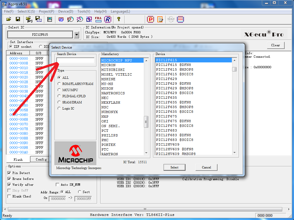
Begin typing the name of the target flash IC, which is “SST39SF010A” in this case. The choices displayed in the right-most “Device” list should narrow down the more characters that you type. Once we’ve completed the chip name, we see that the correct choice has been made for us (i.e. we don’t want to select the PLCC or TSOP versions). Hit the “Select” button near the bottom middle of the window:

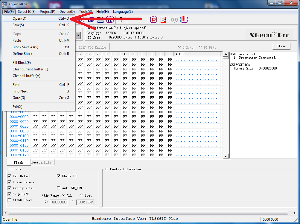
The programmer should jump back to the main window, with the “SST39SF010A” target chip selection visible:

Now we want to load in the BIOS image that Sergey has provided. Click File > Open:
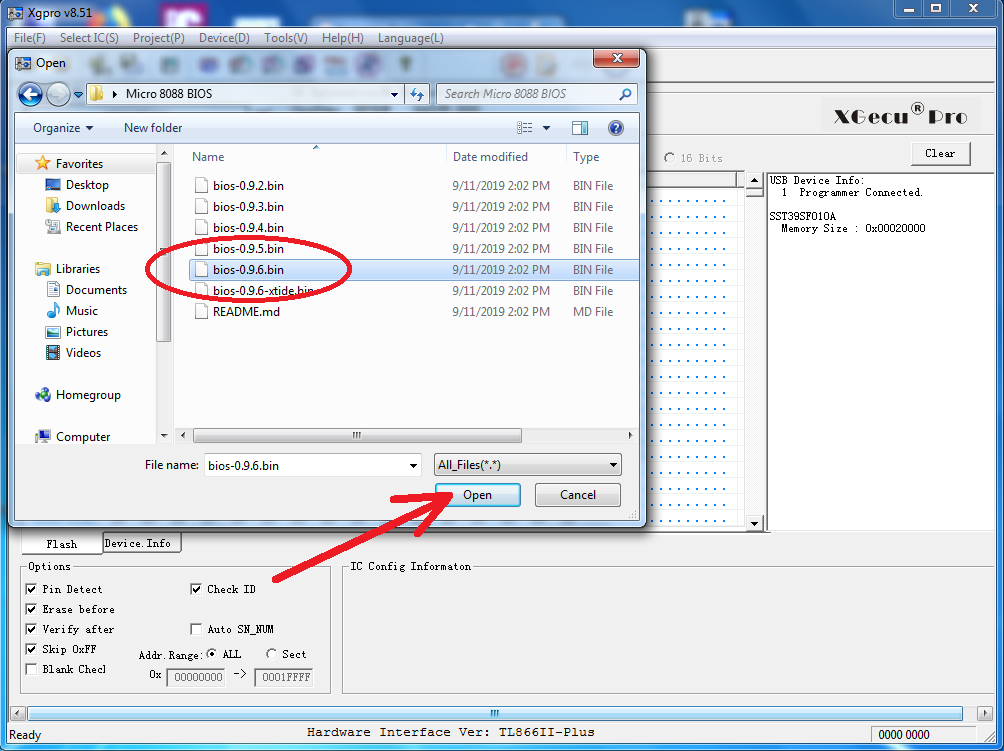
Navigate to the BIOS file, select it, and click “Open”:
The Xgpro programming software will bring up another small window, asking us how it should interpret the BIOS image file. Leave at defaults (i.e. Binary file format, default region) and click “OK”:
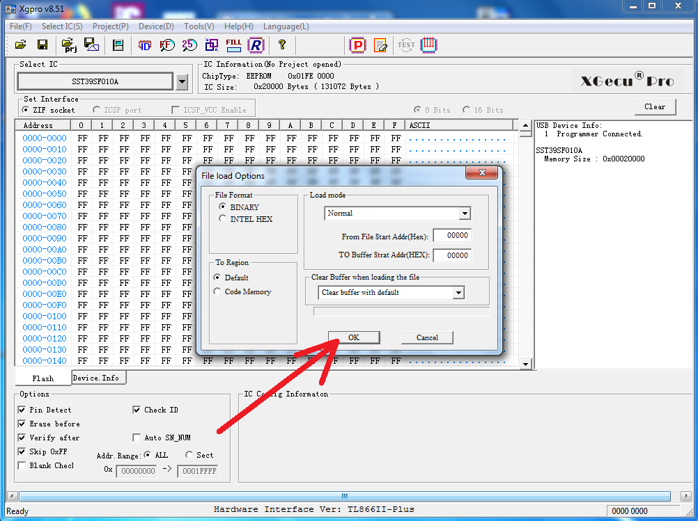
The BIOS file should now be loaded into the programming software. Note: it has not yet been programmed into the IC. We can verify that we have Sergey’s BIOS loaded ready for programming by scrolling down the middle data window to address 0000-C000:

Looks good! Now we want to write it to the IC. Select Device > Program from the top menu:
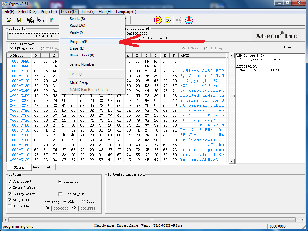
A small window will pop up, inviting us to place the IC into the programmer.
Now, it’s important to get the right orientation for the IC. Look at the top of the IC and locate the “Notch” that is indented into the black plastic at one end (circled red in this diagram as an example):
Make sure the little lever on the green ZIF socket is folded up, and then place the IC near the top of the socket. There is a guide imprinted in the grey plastic adjacent to the ZIF socket showing which way the IC Notch should be pointing:
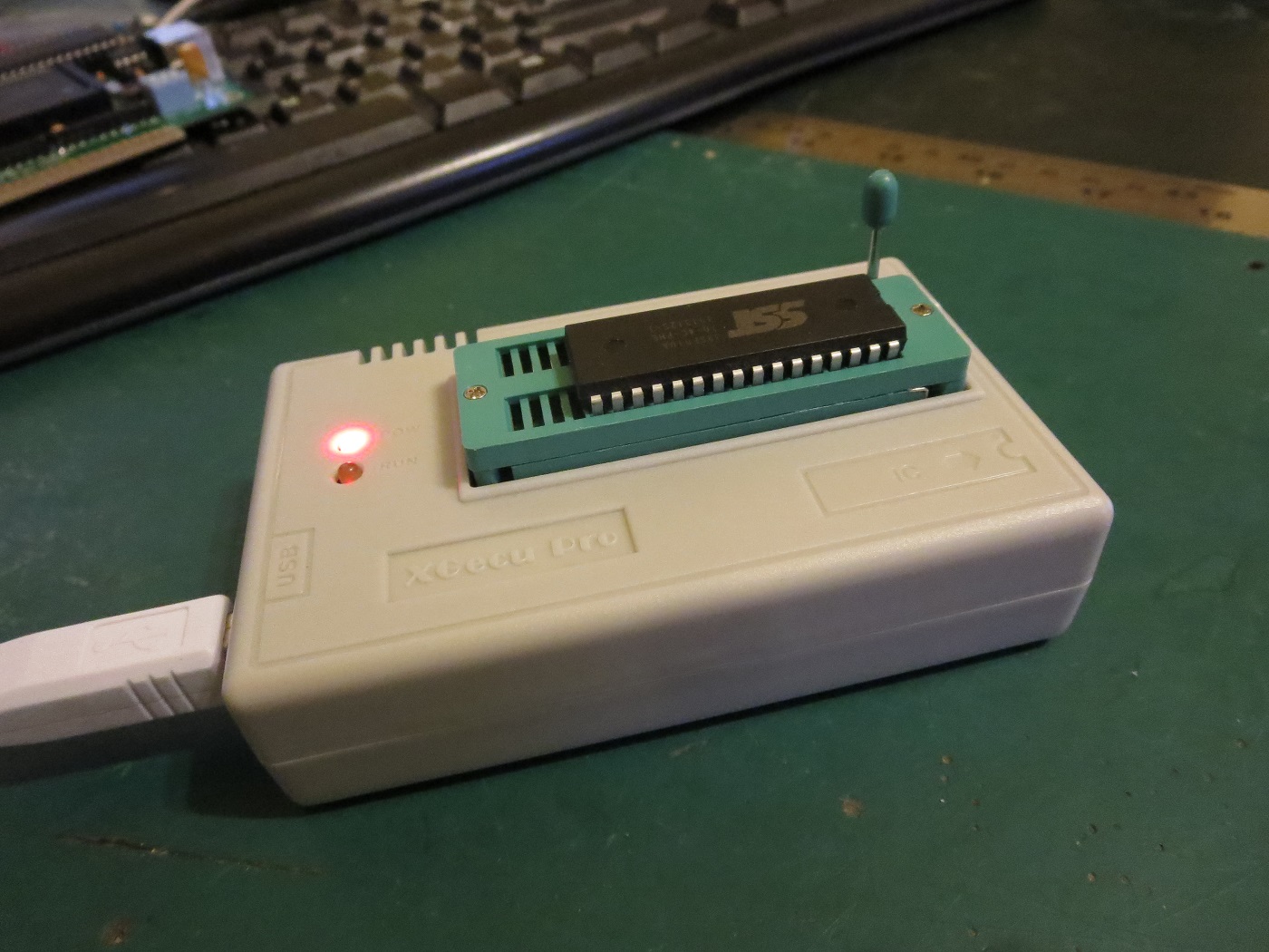
Once it has been placed in the programmer, fold the lever down:
 Now cross-check the programmer window to verify the chip orientation/location against the diagram. Once you’re comfortable, click “Program”:
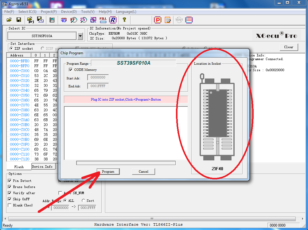
Now, the software will display “Programming Successful” if everything went well. Click the “Cancel” button to close the window:
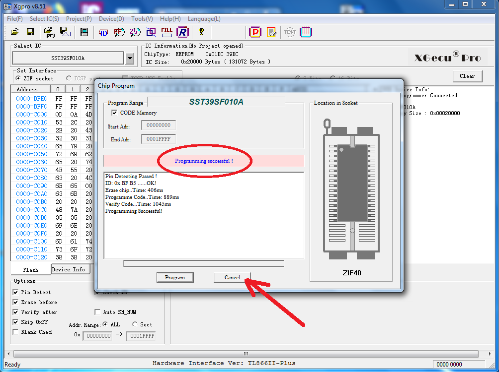 U4 should now have been successfully programmed with Sergey’s BIOS.
If you wish to interrogate the contents of the IC to make sure, you could select Device > Read from the top menu, and follow the prompts to verify the connection of the IC to the programmer, before clicking “Read”. Then close the pop-up window. The contents of the Data window should update to show the contents of the IC that has just been read. You could then scroll to Address 0000-C000 to verify Sergey’s BIOS has been read from the chip.
Remove the chip from the programmer and place it back on the Micro 8088 board.
Flashing U15
U15 is a special chip that is programmed in order to enable the use of a modern PS2 keyboard on IBM XT computers, which use a different keyboard interface protocol. This chip is necessary to allow the FE2010 on the Mirco 8088 to talk to modern PS2 keyboards.
The code that performs the keyboard signal conversion appears to have been an effort of the Vintage Computer Forum. See the AT2XT keyboard converter thread for details. The code also appears on Hackaday.io with credit to Charles P. Guzis.
The firmware for chip U15 (PIC12F629) can be found as an attachment on a post within the Vintage Computer Forum: http://www.vcfed.org/forum/attachment.php?attachmentid=16553&d=1388197270 but note that you’ll need to join the forum to access the post.
Another source appears to be hosted on the Hackaday.io page. The notes for this link state “Intel Hex PIC Firmware – Copyright by Charles P. Guzis, all rights reserved. Chuck Guzis retains all rights to this code, but gives permission to use and modify it for non-commercial, non-profit applications, provided that this copyright notice is reproduced in its entirety.”
Whichever method you use to obtain the AT2XT firmware, the file name you must use is:
- XTATKEY_094.HEX
If you loaded U15 (PIC12F629) into its socket like I did, start by removing it from the Micro 8088 CPU board. I used a pair of flat tweezers to gently pry and work it from the socket, taking care to remove it evenly lest the legs get bent:
Next, connect the programmer to your computer via USB and allow Windows to find and load the necessary drivers it hasn’t done so already.
Next, fire up the Xgpro programming software. You may find that a random chip type has been pre-selected and some data is shown in the central panel. That’s OK. Press the button in the top left where it says “Select IC”:
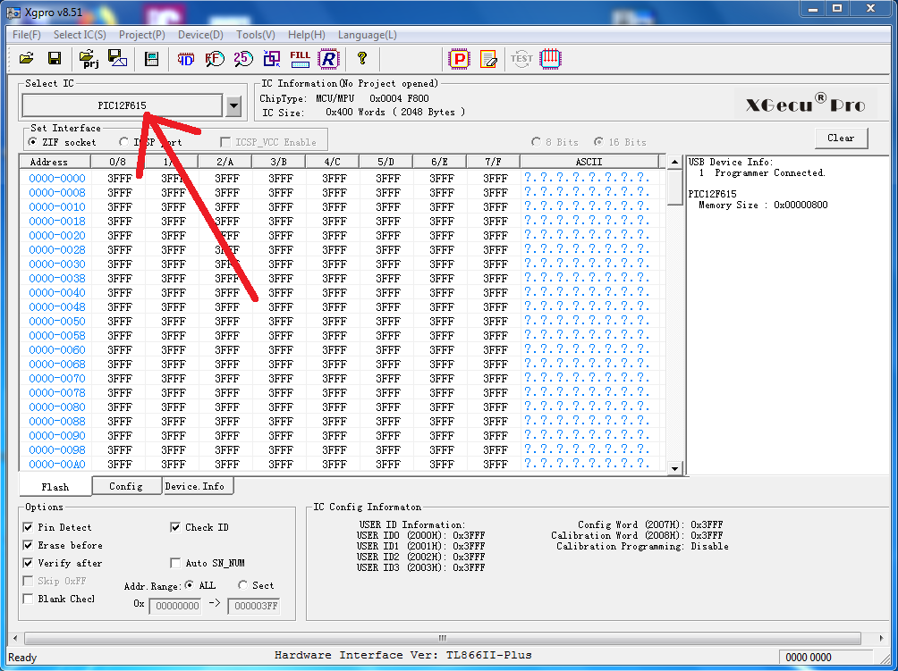
A sub-window will open. Make sure the cursor is active within the small box in the upper left of the sub-window under “Search Device”. Type out the name of the IC which is “PIC12F629”. Select it in the list on the right and press “Select”:

The programmer should jump back to the main window, with the “PIC12F629” target chip selection visible:
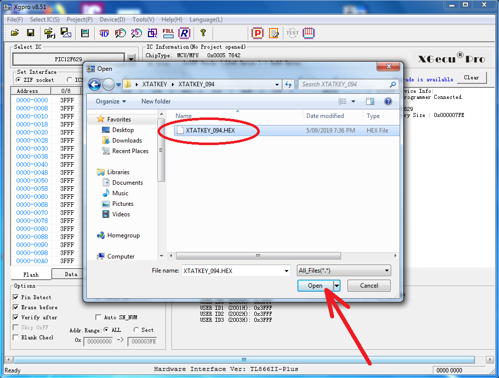
Now we want to load in the XTATKEY_094.HEX firmware. Click File > Open:

Navigate to the file called “XTATKEY_094.HEX”, select it, and click “Open”:
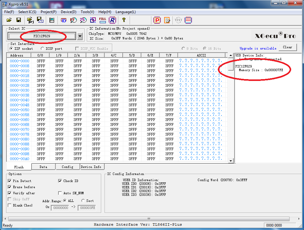
The HEX file should now be loaded into the programming software. Note: it has not yet been programmed into the IC. We can verify that we have some data loaded ready for programming by observing the data window:
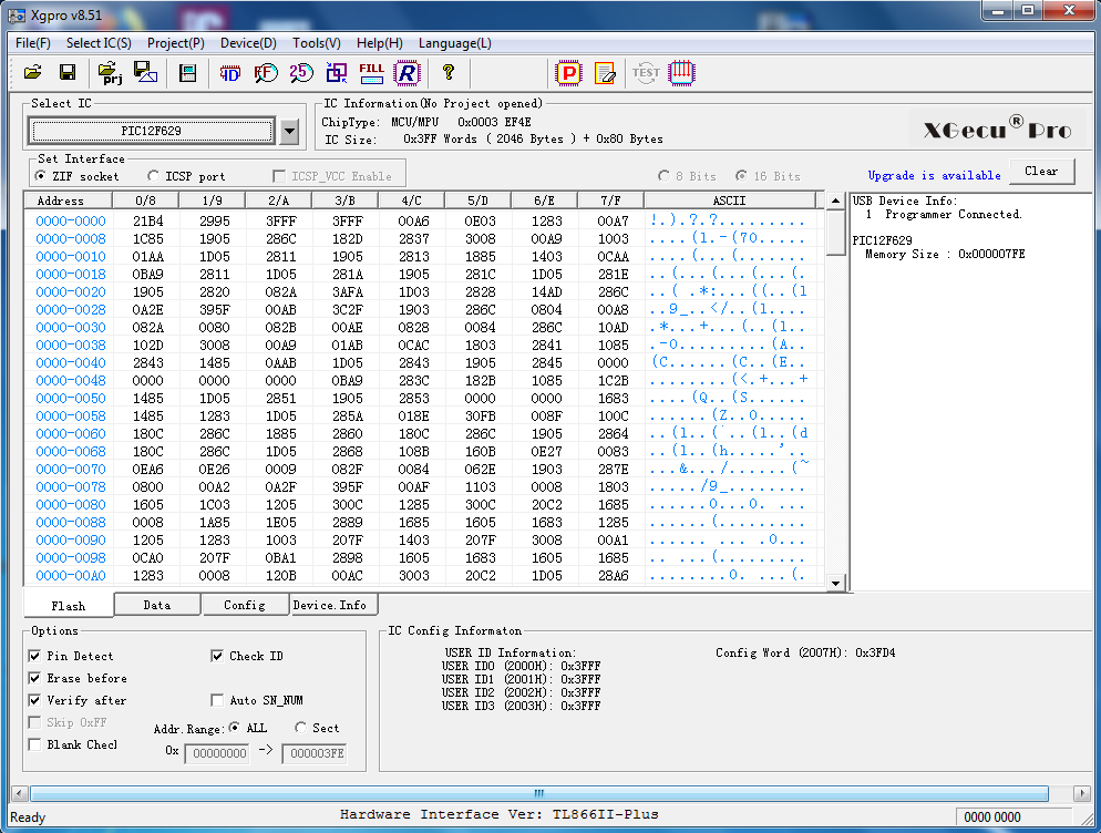
Config word (bottom right) is 0x3FD4. Seems normal? Now we want to write it to the IC. Select Device > Program from the top menu:

A small window will pop up, inviting us to place the IC into the programmer.
Using the IC “Notch” to orient the chip (see U4 programming steps above), make sure the little lever on the green ZIF socket is folded up, and then place the IC near the top of the socket. There is a guide imprinted in the grey plastic adjacent to the ZIF socket showing which way the IC Notch should be pointing. Once it has been placed in the programmer, fold the lever down:
Now cross-check the programmer window to verify the chip orientation/location against the diagram. Once you’re comfortable, click “Program”:

Now, the software will display “Programming Successful” if everything went well. Click the “Cancel” button to close the window:
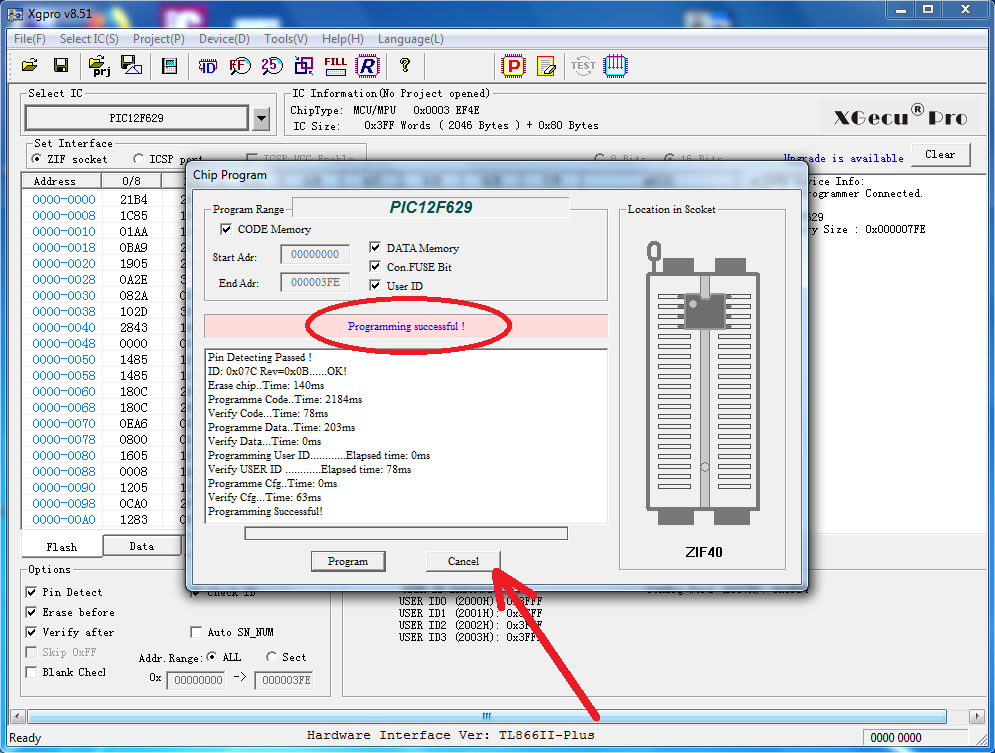
U15 should now have been successfully programmed with “XTATKEY_094.HEX”.
If you wish to interrogate the contents of the IC to make sure, you could select Device > Read from the top menu, and follow the prompts to verify the connection of the IC to the programmer, before clicking “Read”. Then close the pop-up window. The contents of the Data window should update to show the contents of the IC that has just been read. You could then observe the contents of the data window to verify “XTATKEY_094.HEX” has been read from the chip.
Remove the chip from the programmer and place it back on the Micro 8088 board.
Flashing U16
U16 is a special optional chip that allows the Micro 8088 to access a lot more memory than it would ordinarily be able to access if it was loaded with U14.
U16 is an “SPLD” device which is a sort of very rudimentary FPGA. The programming of the SPLD sets up a small network of simplified logic gate structures inside the IC.
Copies of the programming files for U16 are held in Sergey’s Github page for the Micro 8088: https://github.com/skiselev/micro_8088/tree/master/SPLD. They would also have been copied across into the ZIP file of the Github repository, if you followed that step at the start of this post in order to extract gerber files.
There are many different file types presented in the SPLD folder, but we are only interested in:
- micro_8088_prod.jed
If you loaded the SPLD chip U16 (ATF16V8B-15PU) into its socket like I did, start by removing it from the Micro 8088 CPU board. I used a pair of flat tweezers to gently pry and work it from the socket, taking care to remove it evenly lest the legs get bent:
Next, connect the programmer to your computer via USB and allow Windows to find and load the necessary drivers it hasn’t done so already.
Next, fire up the Xgpro programming software. You may find that a random chip type has been pre-selected and some data is shown in the central panel. That’s OK. Press the button in the top left where it says “Select IC”:

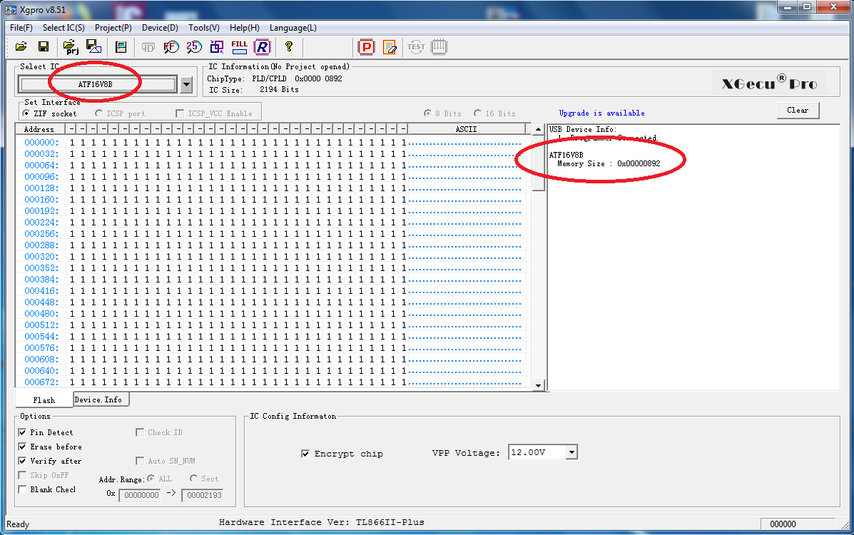
A sub-window will open. Make sure the cursor is active within the small box in the upper left of the sub-window under “Search Device”. Type out the name of the IC which is “ATF16V8B”. Select it in the list on the right and press “Select”:

The programmer should jump back to the main window, with the “ATF16V8B” target chip selection visible:
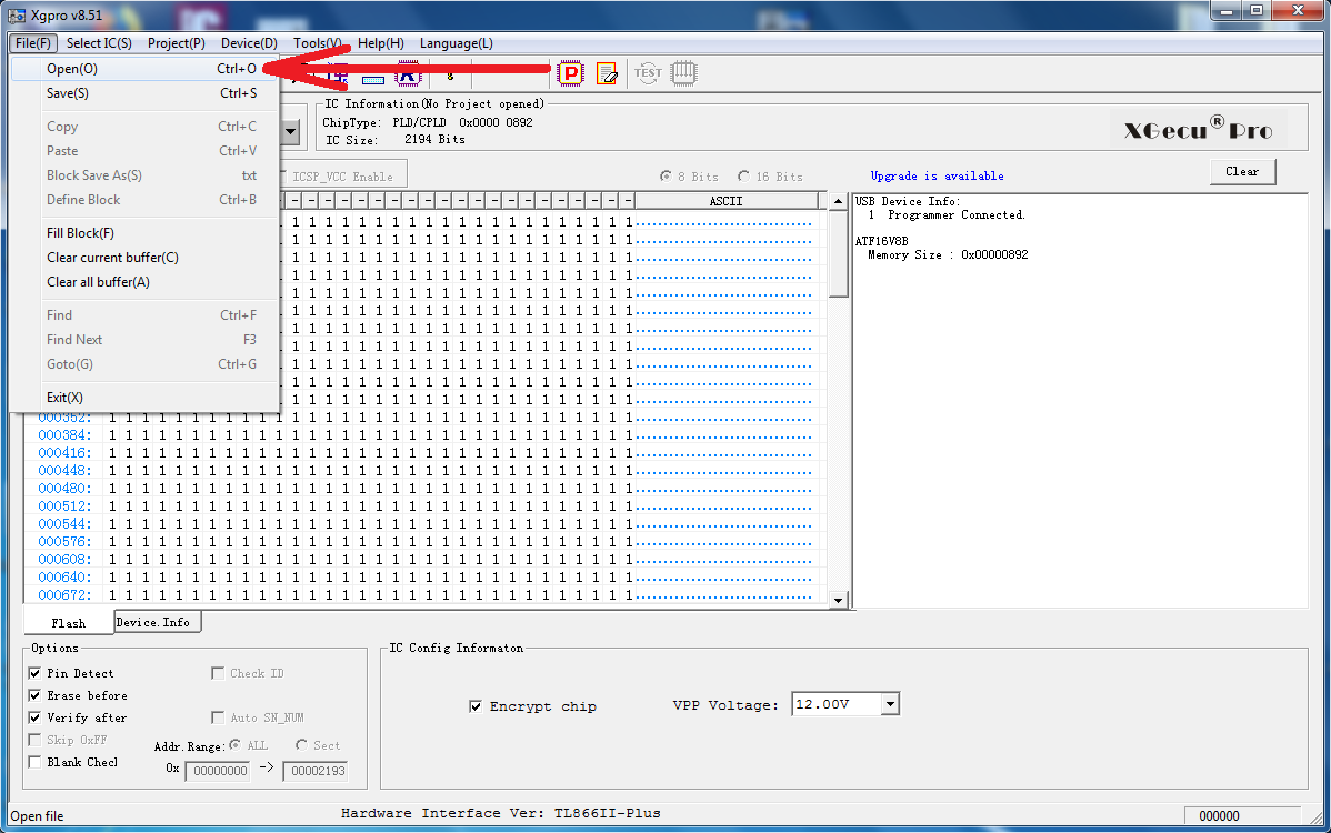
Now we want to load in the .JED file that Sergey has provided. Click File > Open:
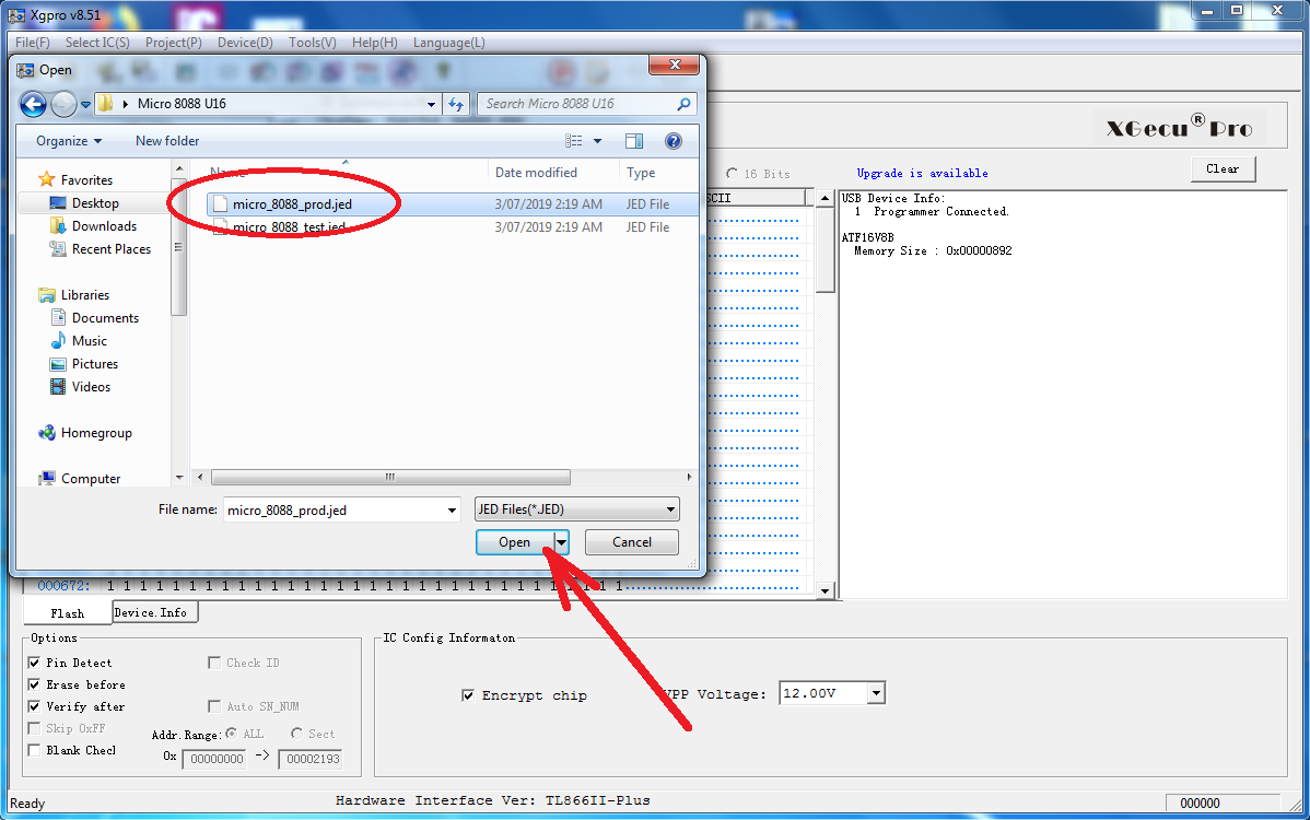
Navigate to the file called “micro_8088_prod.jed”, select it, and click “Open”:
The JED file should now be loaded into the programming software. Note: it has not yet been programmed into the IC. We can verify that we have some data loaded ready for programming by scrolling down the bottom of the data window to address 001536:

A few ones and zeros. Seems good? I think so. Now we want to write it to the IC. Select Device > Program from the top menu:
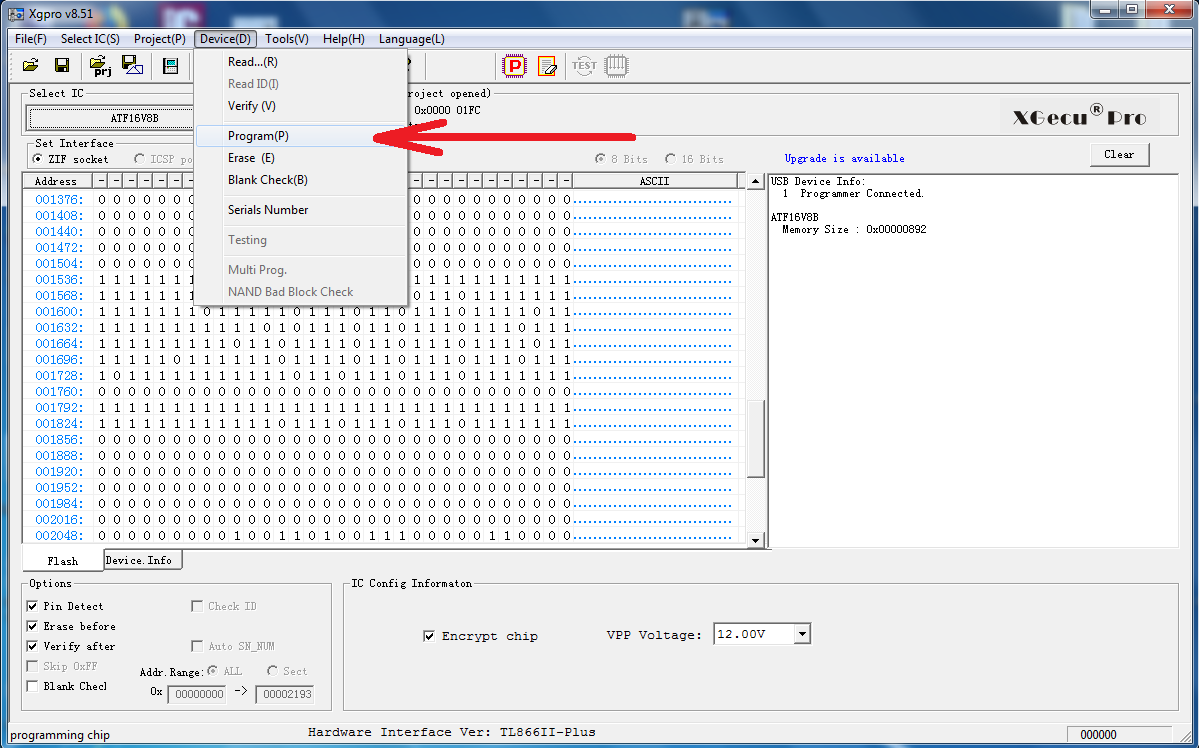
A small window will pop up, inviting us to place the IC into the programmer.
Using the IC “Notch” to orient the chip (see U4 programming steps above), make sure the little lever on the green ZIF socket is folded up, and then place the IC near the top of the socket. There is a guide imprinted in the grey plastic adjacent to the ZIF socket showing which way the IC Notch should be pointing. Once it has been placed in the programmer, fold the lever down:
Now cross-check the programmer window to verify the chip orientation/location against the diagram. Once you’re comfortable, click “Program”:

Now, the software will display “Programming Successful” if everything went well. Click the “Cancel” button to close the window:

U16 should now have been successfully programmed with Sergey’s U16 .JED file.
If you wish to interrogate the contents of the IC to make sure, you could select Device > Read from the top menu, and follow the prompts to verify the connection of the IC to the programmer, before clicking “Read”. Then close the pop-up window. The contents of the Data window should update to show the contents of the IC that has just been read. You could then scroll to Address 001536 to verify Sergey’s .JED file has been read from the chip.
Remove the chip from the programmer and place it back on the Micro 8088 board.
Final Stretch
Goodness! Programming was painful. Now we are at least close to the end of the exercise.
Some things are needed to be done to the Micro 8088 in order to set it up for use:
- If a 28.63636 MHz crystal has been loaded; add a Jumper to the JP2 header. This indicates the use of a higher-frequency crystal to the FE2010. If a 14.31818 MHz crystal was loaded, then leave this jumper off (open).
- If U14 was loaded instead of U16; add a Jumper to JP3 and JP4. This sets up the memory to be handled by the FE2010.
- If U16 was loaded instead of U14; do not add any jumpers to JP3 and JP4. Ensure they remain open.
- Again; ensure that U14 and U16 are not both installed. Choose one or the other.
- Do not add a Jumper to JP1. This is to do with the mapping of flash ROM and the odds are it can be left open for now.
- If you wish to hear the on-board speaker sounding; add a jumper to the lower two pins of the P2 header (adjacent the speaker). I.e. the two pins closest to capacitor C4.
- Move all switches in the SW3 switch bank to the off position for now.
- If you wish to use a CGA card as the graphics card for the Micro 8088 (as I do), then set the first switch of the SW2 switch bank to the on position. Set the second switch of the SW2 switch bank to the off position. Other graphics cards (MDA/Hercules, EGA, VGA) can be chosen with different switch combinations.
- Because I don’t know what it does, I set the third switch of the SW2 switch bank to the off position. This apparently disables keyboard 0xE0 scan code pass through. Hope I don’t need that.
Finished
Finally! We have done all we can to prepare for the use of the Micro 8088. As a recap:
- The blank PCB boards were procured.
- The parts were ordered from a combination of Mouser and Utsource.
- The boards were assembled, with various tips provided based on what I found during the process.
- The chips were programmed after much trial and error, and frustration (U4, U15 and U16).
- The board jumpers and switches were set in preparation for first run.
In theory, the BIOS should be able to take control of the CGA card and cause it to display some data. The plan from here is to plug the Micro 8088 board and my repaired CGA card into the backplane and see if I can see the BIOS screen.
But this post is long enough already. I’ll save the test run for a future post.
Hope you enjoyed, and see you soon on the next instalment of this adventure in retrocomputing.