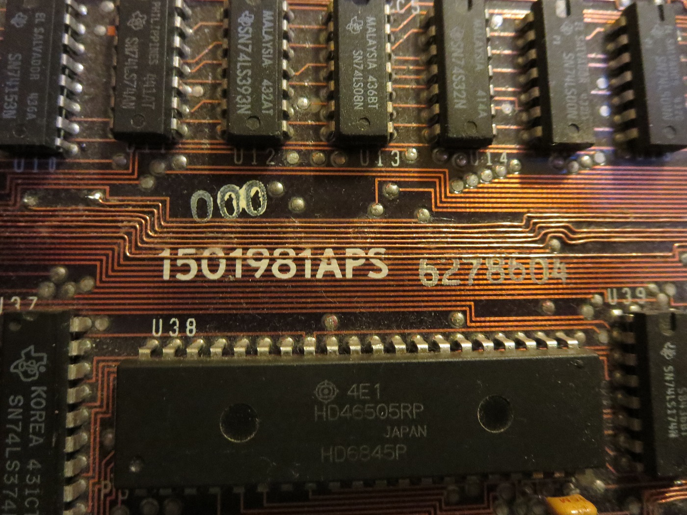
Following on from My Introduction to Retrocomputing, I had found myself in possession of an IBM CGA card numbered “1501981APS”. At some point in my childhood, I had damaged the card by pulling traces off the PCB. I’m still annoyed at myself for that. Nonetheless, I still want to repair the card and attempt to get it working with Sergey’s Micro 8088.
So what sort of damage are we dealing with? Quite a lot. Here’s a photo showing some of the damage, with many traces missing (blue arrows):
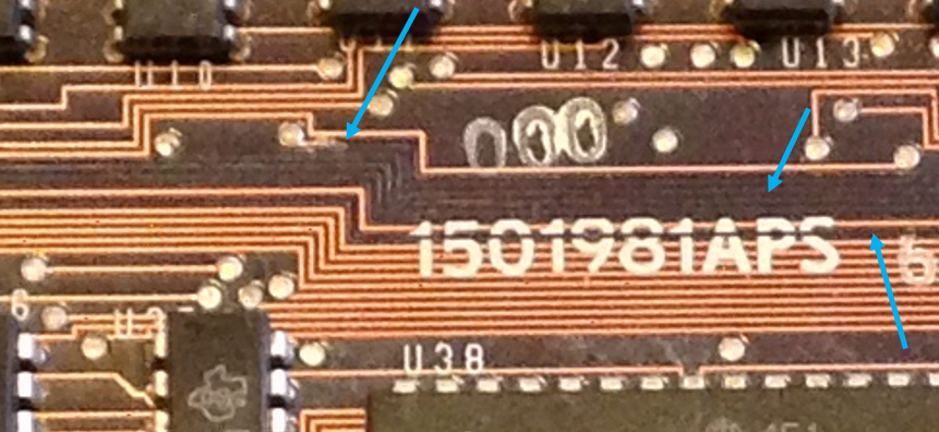
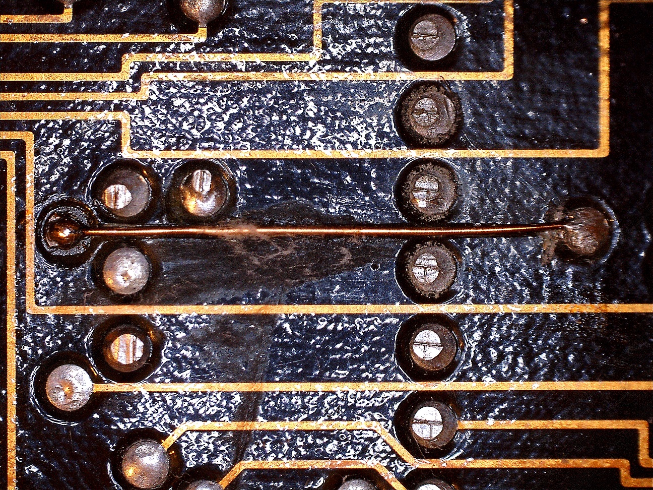
And a close up view, typical of many traces that have been pulled off between through-hole pads:

The damage was caused by mechanically severing the copper traces near through-hole pads, and then rolling them up vertically to form a tab, after which they were grabbed and pulled from the board with pliers or tweezers. The traces were essentially de-bonded from the PCB substrate during this process.
As the traces came away from the board, they also took away the solder-mask that was covering them. The paths of each old trace were made visible by following the missing solder-mask channels that were left behind. On this damaged CGA card, fifteen traces had been lifted, each on average 200 mm long. That’s a lot of repair work.
In the end, I settled on a particular technique for repairing these traces. The technique relied on the use of very fine enamelled copper wire (sometimes referred to as magnet wire) to replicate each trace on the board.
I started by choosing a 0.25mm diameter enamelled copper wire:

Next I chose which particular trace I was going to repair. I measured the length of the trace and then added approximately 50 mm for wiggle room. I measured out that amount of enamelled copper wire and then cut from the spool.
The cut end of the enamelled wire cannot be directly soldered as the full length is protected by the enamel:

Before soldering the wire to the board, we have to remove the enamel. There are a few steps required to accomplish this.
First, place a blob of solder onto the iron:
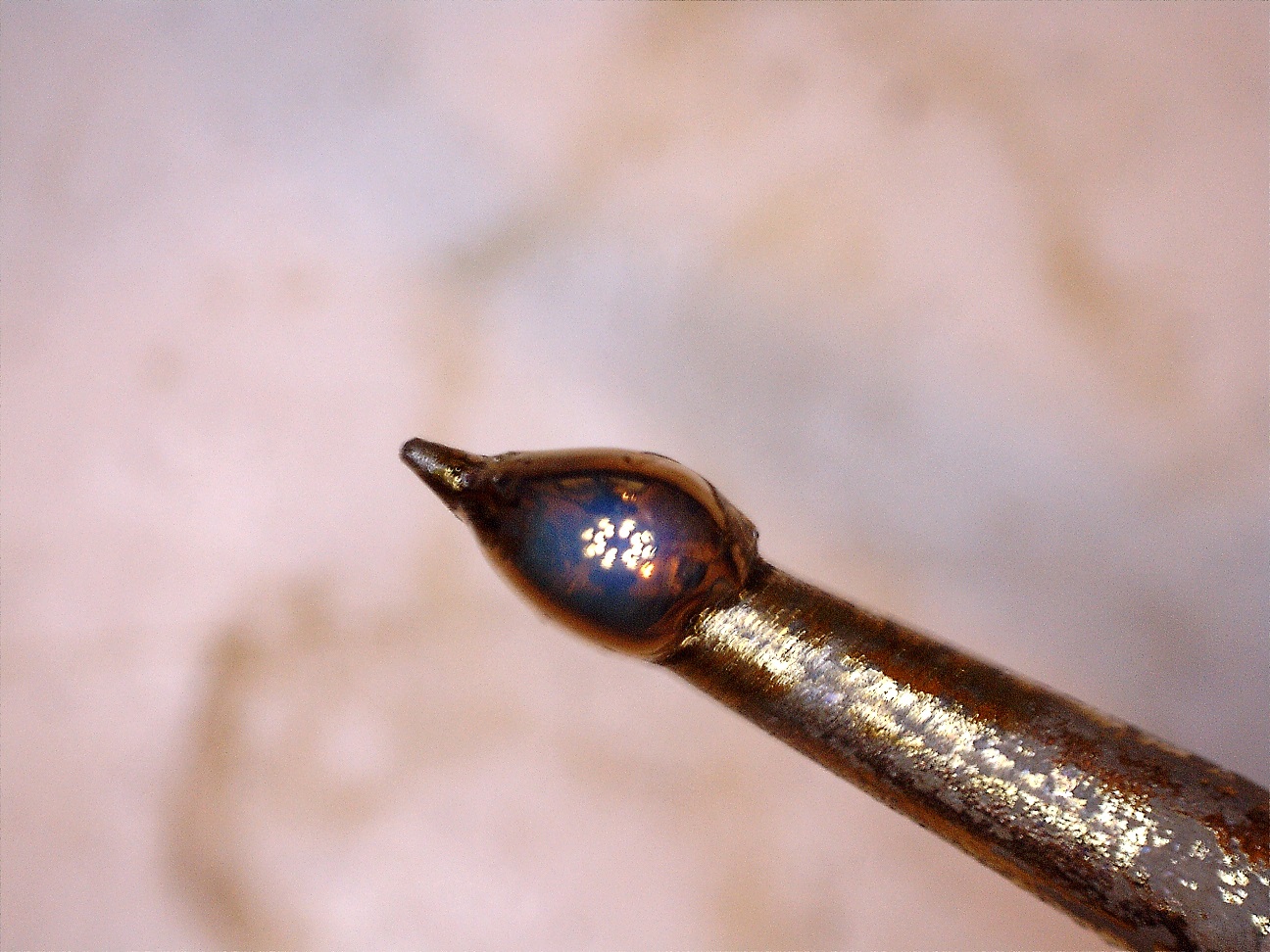
Then move the end of the enamelled copper wire onto the solder blob (the blob had oxidised slightly while I arranged the photo):
 Then submerge the end of the wire into the blob:
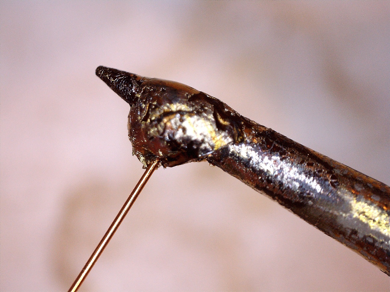 Hold the wire in position for half a minute or more, and rely on the heat of the iron to melt the enamel from the end of the wire. Removing the wire from the blob, it should be obvious that the enamel has melted, and in its place the copper has been tinned:

If it doesn’t look like the enamel has been removed, repeat with a fresh solder blob and more submersion time.
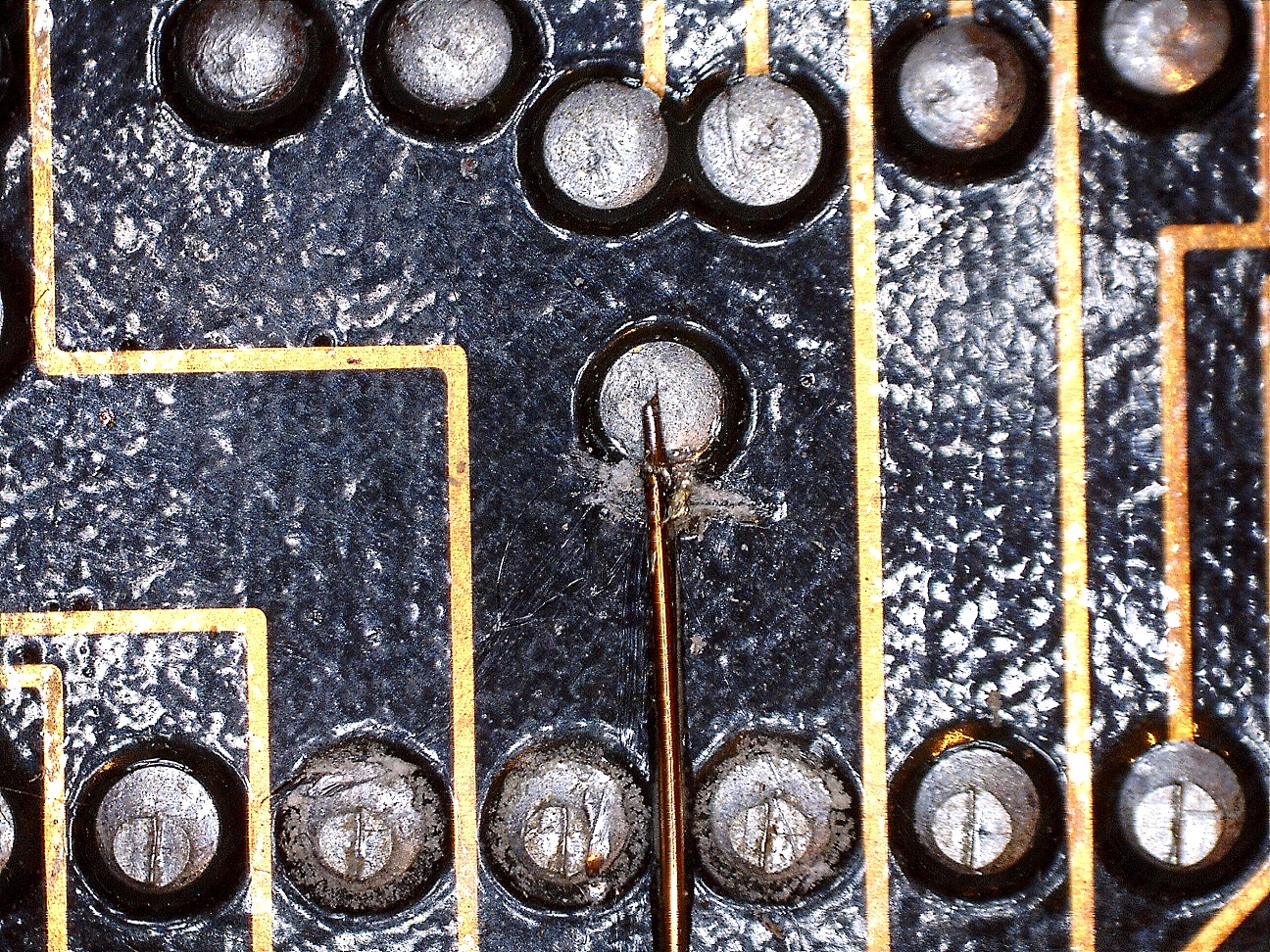
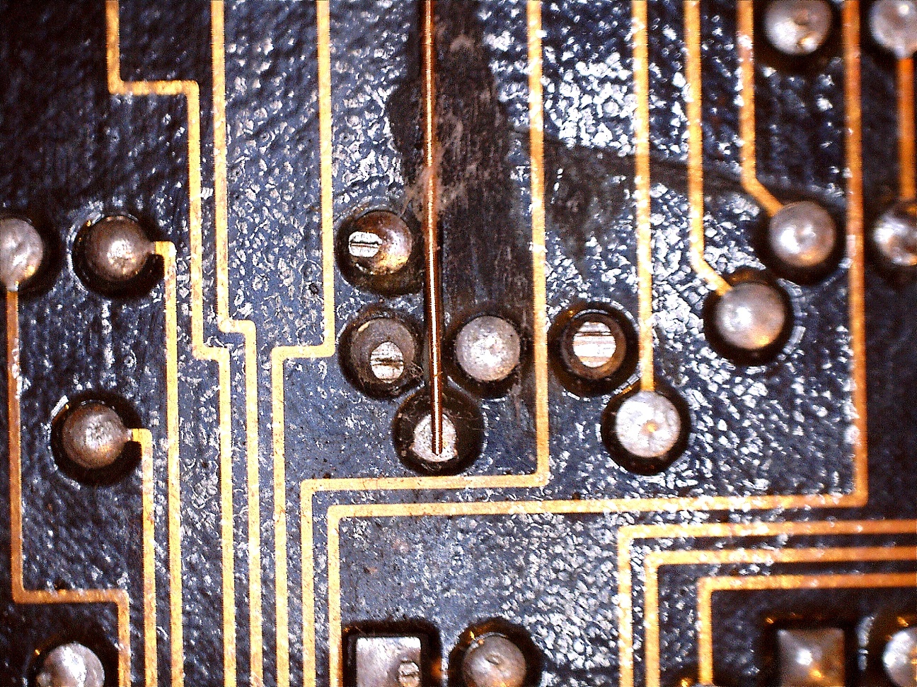
Once the enamel has been stripped, align the end of the wire over the adjacent through-hole pad:
Apply the soldering iron and press down on the end of the wire:
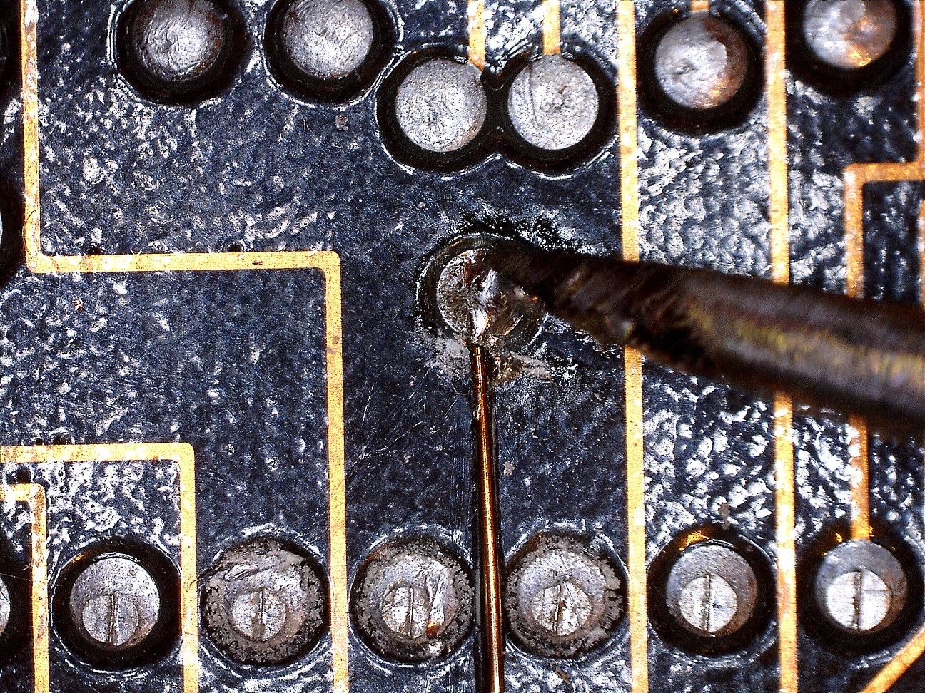
The solder should melt, covering the end of the wire. While the iron is still applied, align the wire so that it follows the line of the old PCB trace. When happy, remove the iron and let the solder solidify:

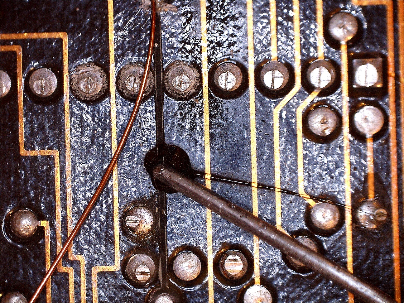
The loose end of the wire should now be pointing vaguely in the direction of travel of the old PCB trace:

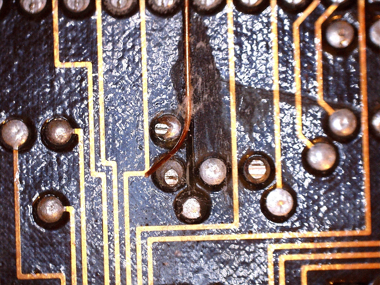
For the full length of the missing trace, we want to periodically super-glue the wire into the channel formed by the absent solder-mask.
Every 15 mm or so, add a small dab of super-glue into the missing solder-mask channel (I’m using the end of a paperclip to carry the glue into place):
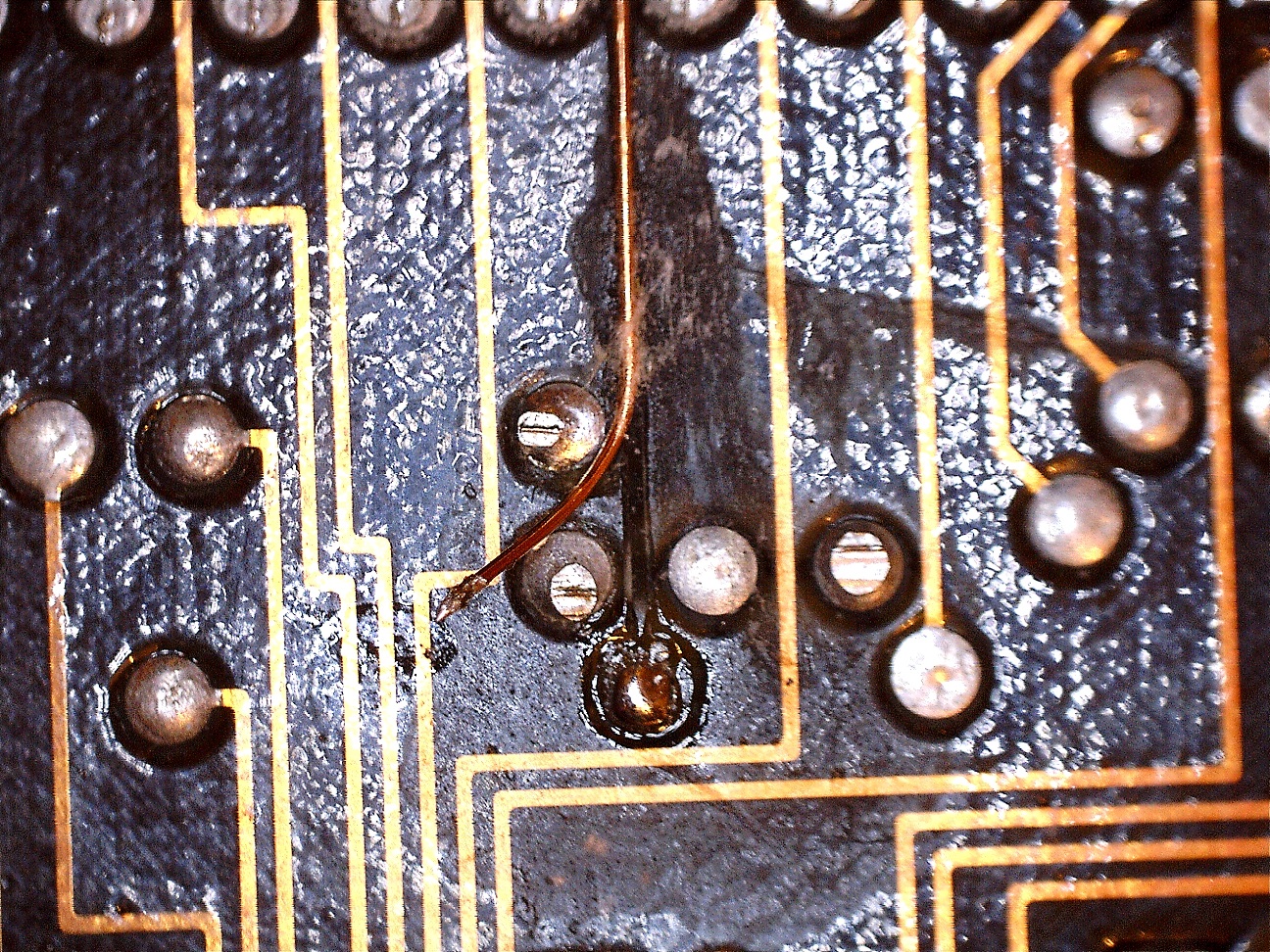
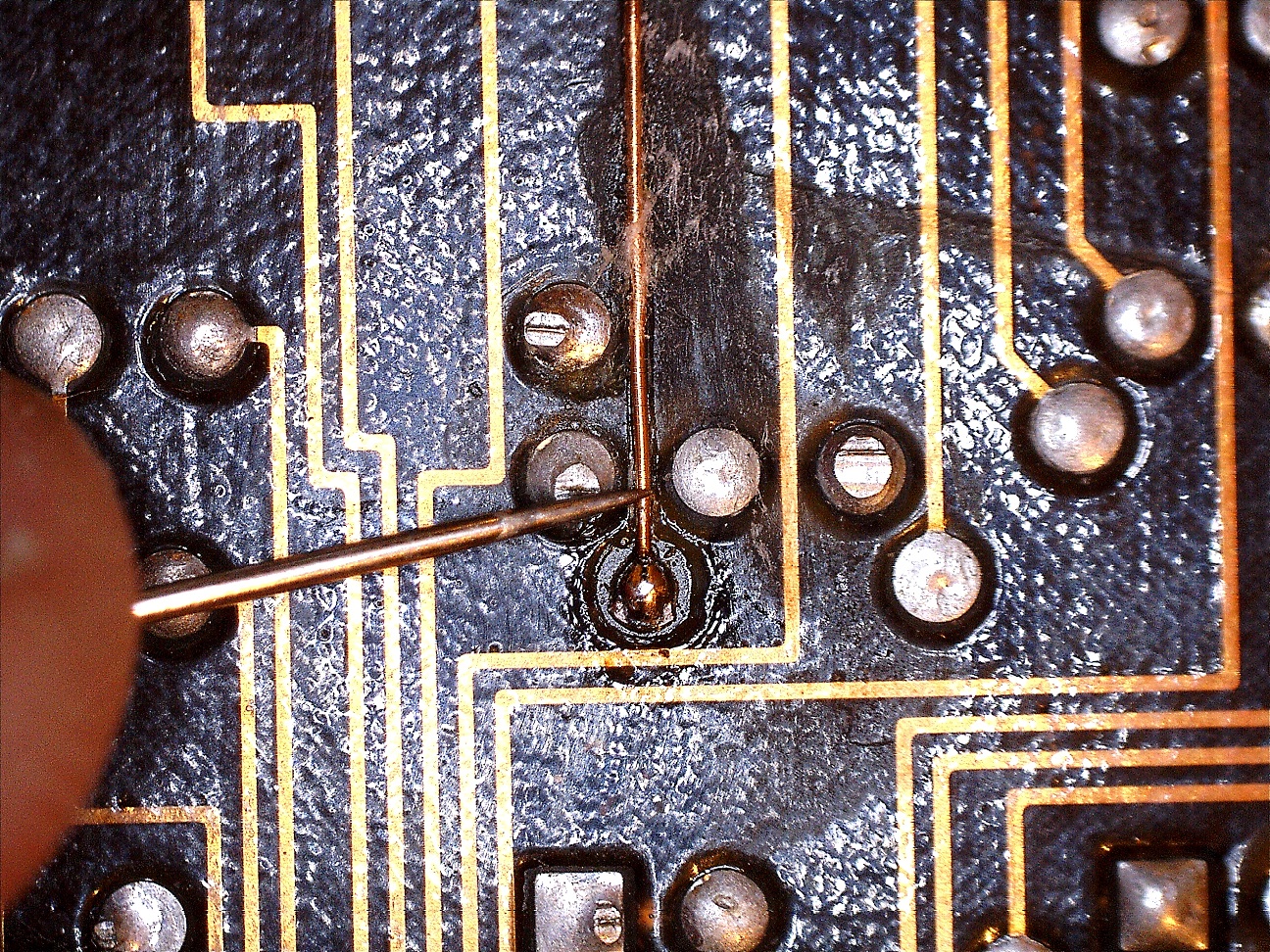
Align the wire into the channel and press down with some kind of tool or implement to avoid getting super-glue all over your fingers (I’m using the plastic shaft from a cotton-swab):
 Once the wire has dropped into the channel, hold in position for half a minute or so until the glue catches. You may also wish to slide the pressing tool up and down the wire, over the blob of super-glue, to encourage it to stick. After it has stuck, you’ll be left with the wire secured in the solder-mask channel:
 Note that I’ve used way too much glue in this instance, and I’ve also made a mess by trailing glue over adjacent traces. It’s worthwhile cleaning the excess glue off as it has a tendency to out-gas and form a white chalky buildup around the area.
The wire after trying my best to clean with tissues:
The process of super-gluing should be repeated every 15 mm or so along we wire, over the majority of its length. The wire should be bent with sharp tweezers to follow any change in direction in the solder-mask channel. At some point we will reach the end of the solder-mask channel. The gluing should be stopped approximately 15 mm before the end of the channel.
The wire should be aligned over the through-hole pad that forms the end of the trace:
using very sharp side-cutters, the trace should be cut to length:

Leaving approx 2/3 of the pad diameter as overlap in this case:
Then the wire is bent up and away from the board, to give access to the pad below:
 Although this step may not be strictly necessary; the pad is re-tinned with solder:
 And the wire end is stripped of enamel by submersing it in a blob of solder on the iron tip:

If not successful, repeat the solder blob submersion until the wire end has been visibly tinned:
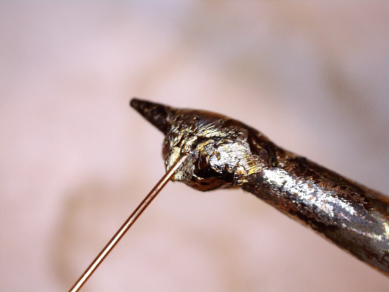
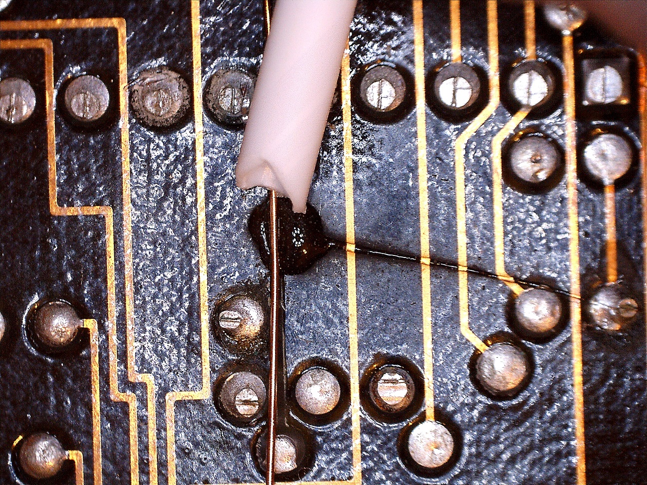
 Then, using a fine implement like a pin or a toothpick, bend the wire end back in place over the pad. Press down on the wire with the implement a small distance from the pad, and apply the iron to the pad:
 The melted solder will flood and surround the wire. Manoeuvre the wire until it rests within the solder-mask channel, then remove the iron and allow the solder to solidify:
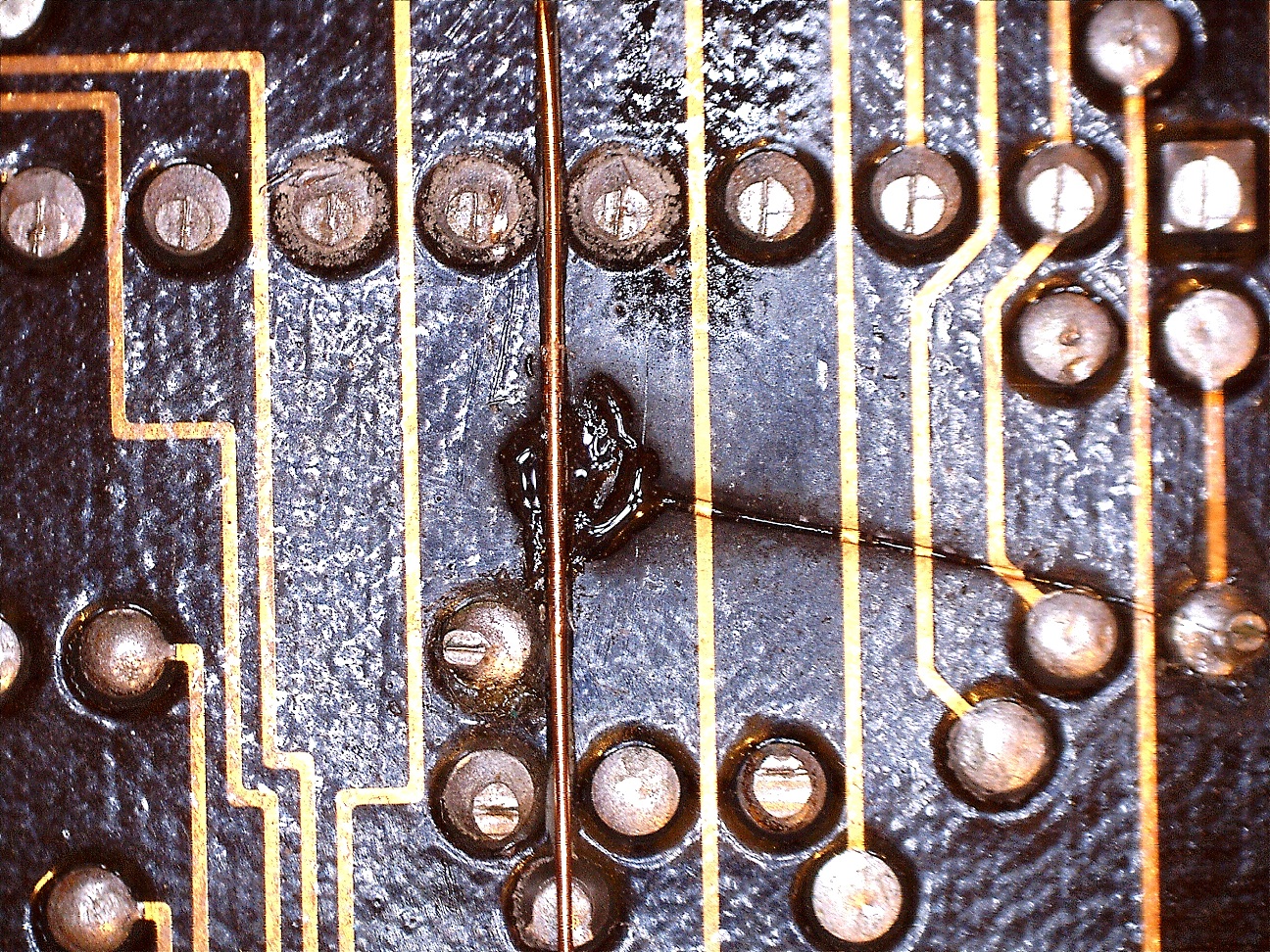
Once solidified, remove the implement:
 And that’s it! One trace has been repaired.
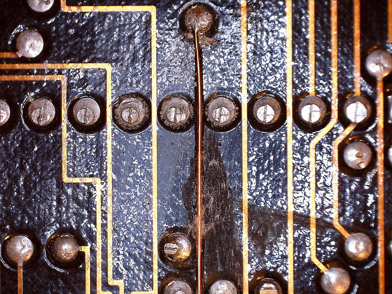
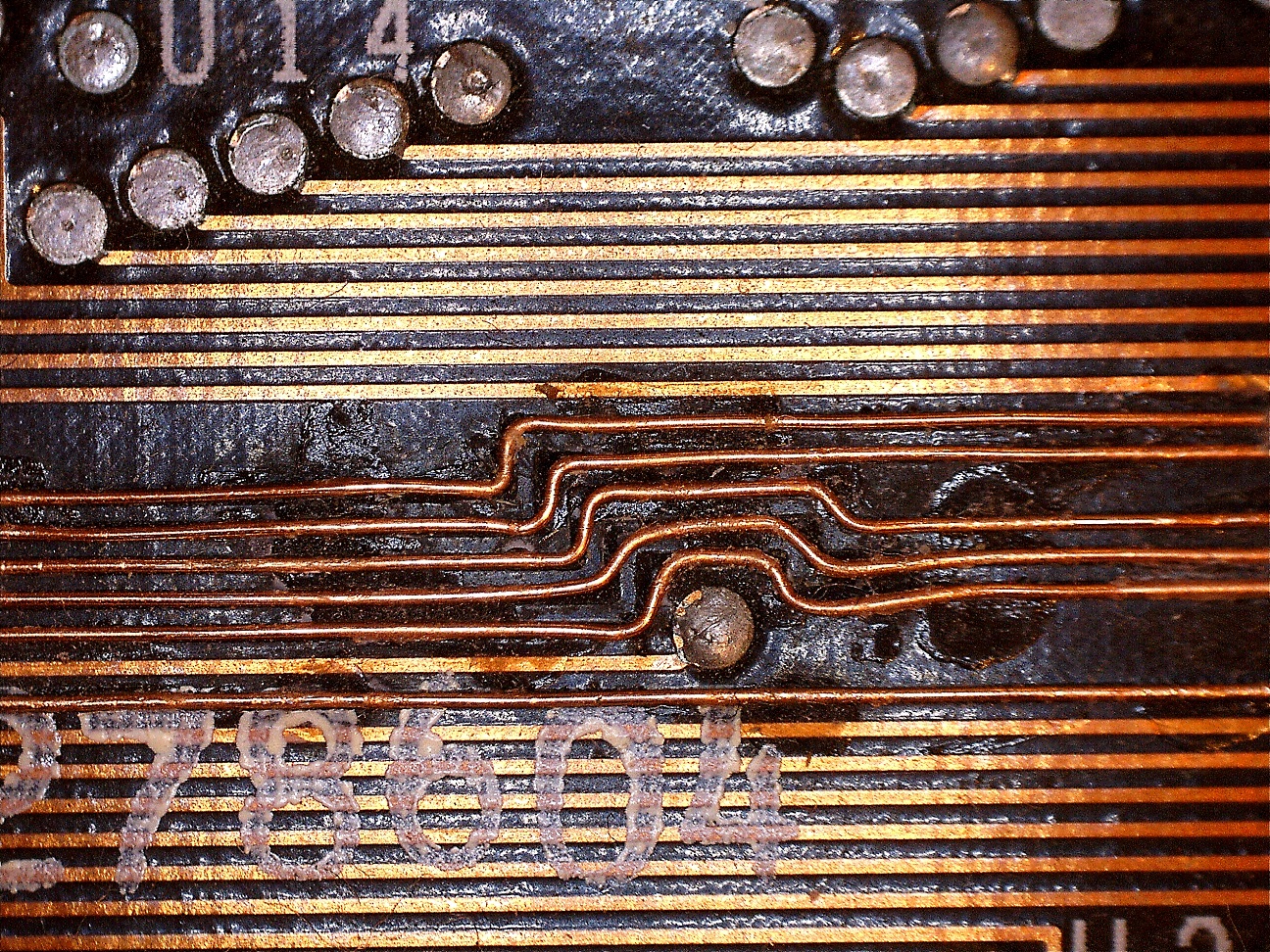
In this particular example, the trace being repaired was quite short and simple. Here is a photo of the total repair:
 This process was repeated fourteen other times over the course of many days to repair all of the damage incurred to the CGA card traces.
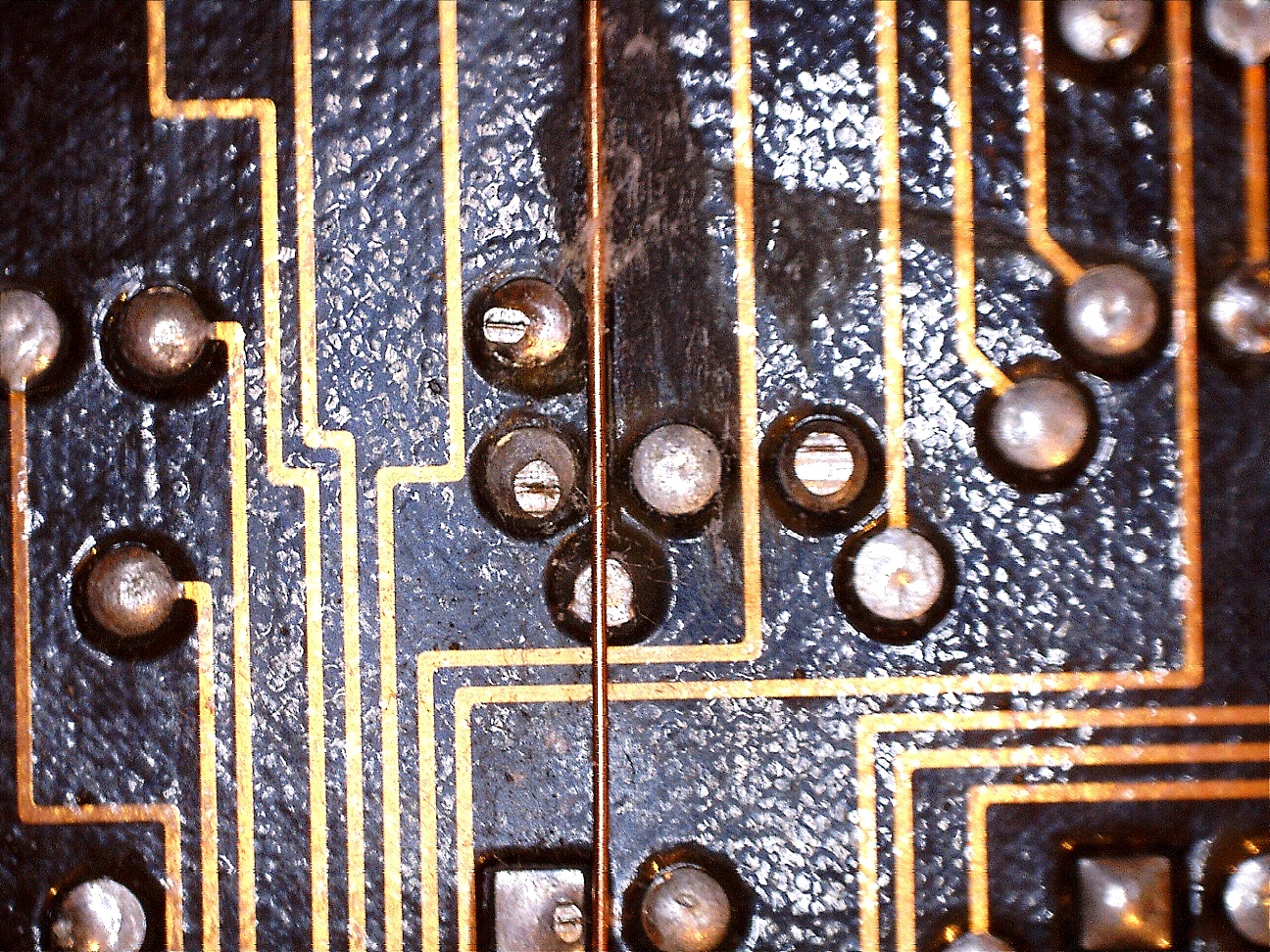
Some photos of the intricate routing required with the enamelled wire:


And one “super fun” trace that had only been severed a short span, far from the through-hole pads (near centre of photo, near U39 and U40 bottom edges):
The same trace following repair:
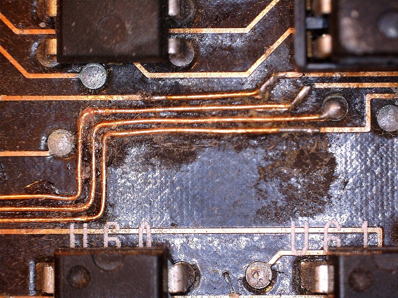 The strategy for this short piece was the same as above, except that a length of the preexisting trace was exposed on each side of the missing segment by scratching off the solder-mask and tinning the trace with solder and plenty of flux. I’ve had to do the same on the trace second from top, as this did not end close to a through-hole pad. The sequence of steps above will work well provided that the solder-mask is scraped away and the traces are well tinned.
An overview photo showing the extent of trace repairs:
 Although you might think the repair is finished at this point, there are more very stupid things that I discovered that I had done to this board when I was young:
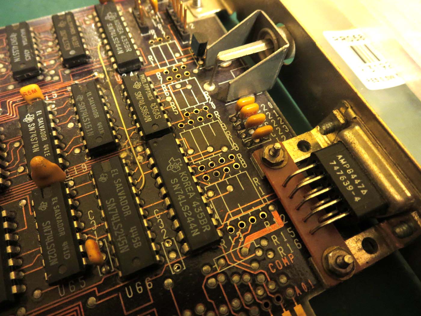
Yes. I had removed all of the resistors on the end of the board. As it turns out, these resistors are critical to the digital and composite video generation circuitry. I won’t have any chance of seeing video output if these resistors are not replaced.
Thankfully, I discovered that the schematics to the IBM CGA board (or at least one version of it) have been scanned and placed online. The composite video resistors can be seen on page 36 (schematic sheet 5 of 6). The digital video resistors can be seen on page 37 (schematic sheet 6 of 6).
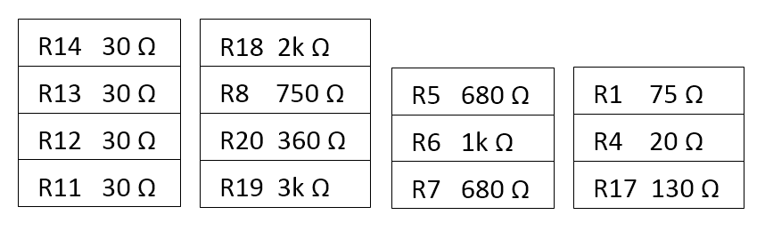
Using the schematic and a multimeter, it was possible to deduce the resistor names, values and relative locations (looking from the connector-end of the board):
In addition to this, I discovered that I had removed capacitor C32, which is a 47pF smoothing cap for the Horizontal Sync output of the digital video (RGBI) connector. I replaced it with a ceramic equivalent.
I found one other resistor missing; R2 which is situated below and to the left of the CRTC controller (U38):
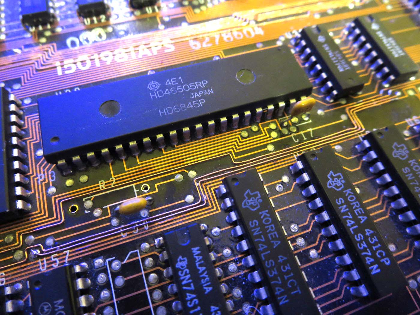
As it turns out, this resistor is connected to the character ROM chip, and serves no apparent purpose based on the schematic (See page 33, schematic sheet 2 of 6). I replaced it anyway with the schematic value of 2.2k Ohm.
After buying all resistors as close as possible to the values required, I soldered them all in place. I had difficulty finding some resistor values, so I used the next available values instead (e.g. 690 Ohm instead of 680):
 And that’s finally it! all damage seemingly repaired.
Unfortunately I won’t be able to test this card until I solder together the rest of the boards required to make a functioning retrocomputer.
So, next step: making Sergey’s Micro 8088 processor board and backplane board.