The last post in this series covered aspects of the initial schematic design of the Retro-CGA. This post will crack on with the initial board design, using the magic of pictures to show the detail of the board build-up.
I hope that you enjoy seeing the progress thus far on the Retro-CGA.
Starting Small:
For the physical shape of the card, I’ll be using the ISA board dimension drawing that I created when designing the ISA POST card. This drawing is a combination of the card specifications found within the IBM 5150 Technical Reference Manual, with additional references/changes to accommodate the Keystone 9202 mounting bracket that is commonly used in modern ISA designs.
The first step was to define a closed-loop shape on the “Edge.Cuts” layer to define the board outline in Kicad. After this, the ISA card edge footprint and the Keystone 9202 footprint were imported and aligned:

The card edge footprint and the keystone bracket footprint have guide marks drawn on the “Eco1.User” layer to help align the “Edge.Cuts” layer around the card edge connector.
The 3D viewer function in the View menu can be selected to see a helpful rendered image of the board:

Hooray. I can imagine the completed card already.
Ordinarily, when the board design is updated from the schematic, every single package will be dumped in to the board at once. I’m hiding a great deal of components on the outside of the board until they are ready to be brought in. I’ve also turned off the ratnest “airwires” to de-clutter the workspace.
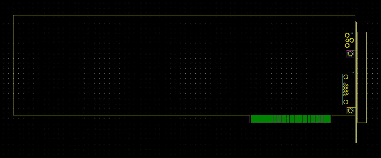
Next step, adding the RCA jack and the RGBI connector. I’ve gone with a Keystone 589 for the RCA jack, and a Kycon K22X-E9S-NJ for the D-Sub that forms the RGBI connector. In retrospect, the RCA part could be changed to a type that is more numerously held in stock, but this can be done later. The board with the components added:
And with the 3D view:
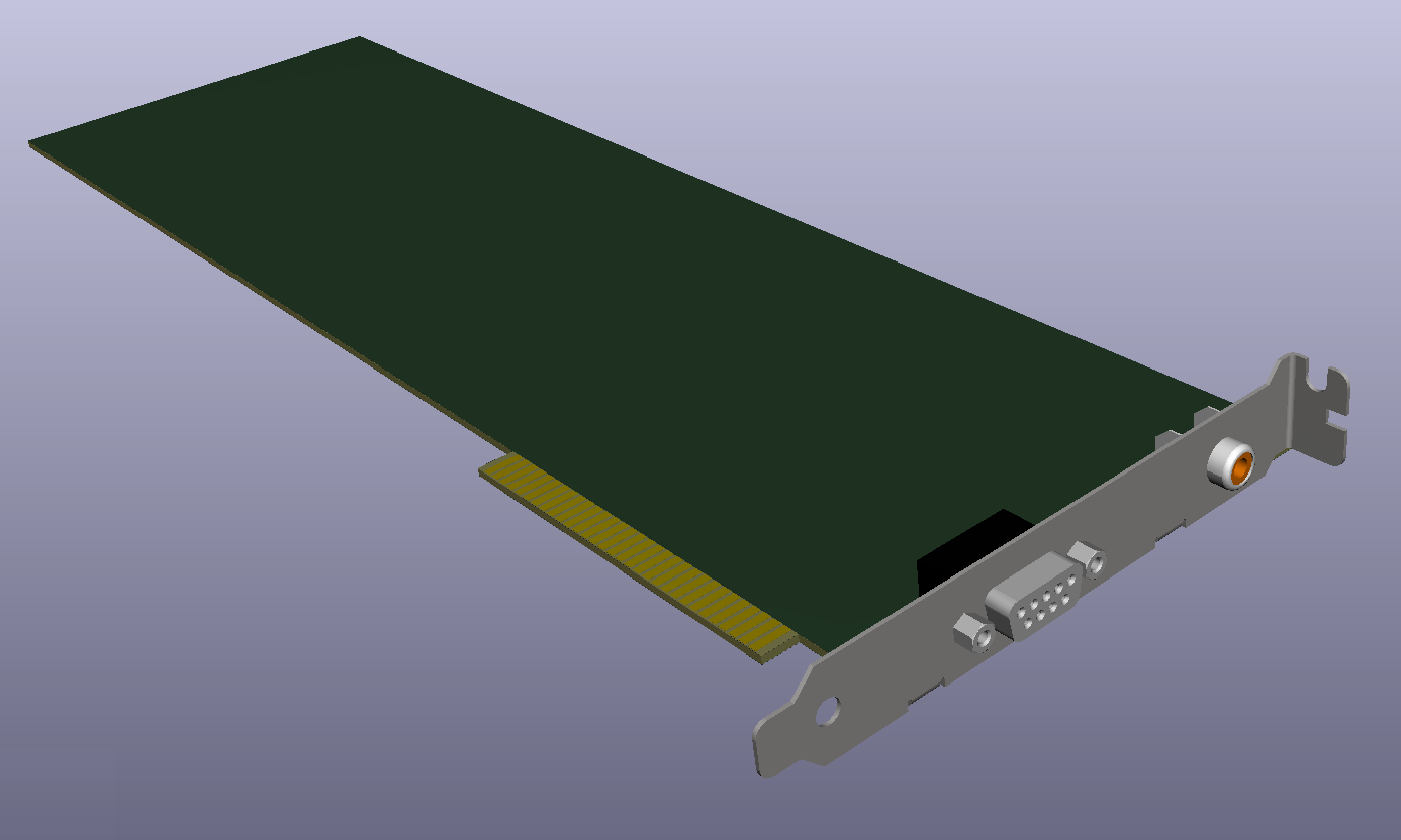
Next, modifying the keystone bracket 3D model to feature through-holes for the composite video jack and the RGBI connector:
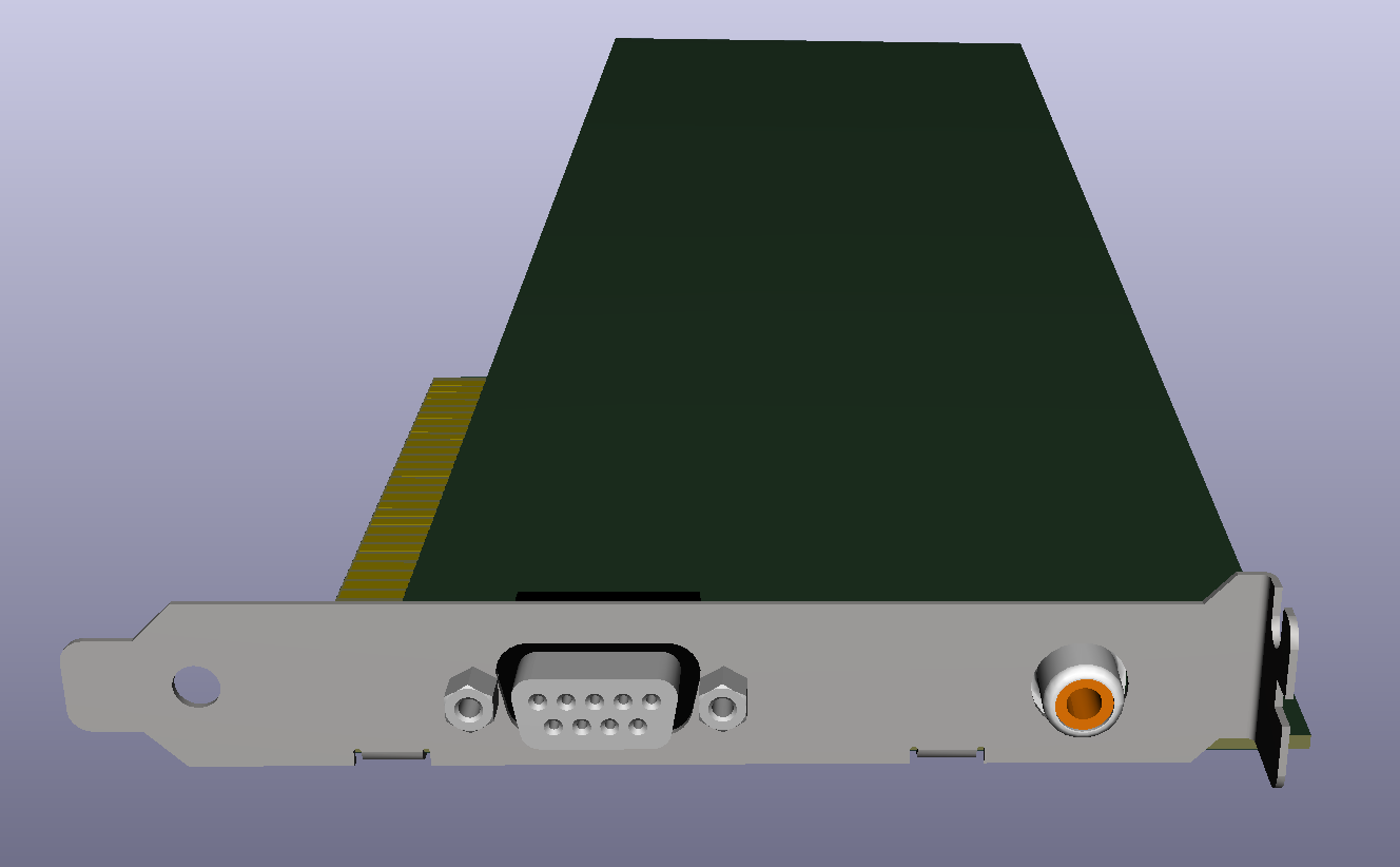
Much better.
Next, all of the IC packages are arranged inside the board area. This took a lot of time. I’ve set the grid spacing at 2.54mm to simplify alignment of the IC packages. Quite a bit of tweaking and fine adjustment is expected to be necessary later on when the trace routing starts. Again, net wires have been hidden for now because they are too distracting to be useful at this stage:

Straight away, there should be some noticeable differences with the original CGA card. It should be noticeable that the video memory chips have been rotated and grouped into two banks of four, and the U58, U59, U60, U61 and U101 ICs have been rotated and aligned. This is in service of removing the “re-entrant” board edge that would prevent this card from being plugged into a 16-bit ISA socket. Unfortunately for me, this choice will greatly complicate the board routing due to the lost vertical area. The more modern character ROM chip can also be seen taking up a lot of room mid-left of board. Chip placements have been inspired by the original CGA to give it the same visually pleasing aesthetic while still allowing for the different changes being made.
More time was spent aligning the silkscreen IC names. In a 3D view:

The next step was to arrange the capacitor and resistor footprints, as well as the composite video output transistor:
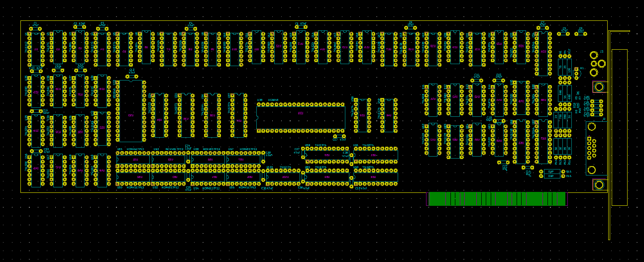
Again, the silkscreen names were adjusted at this stage while the board is not too cluttered with traces. In a 3D view:

After getting sort-of-comfortable with the IC layout, giving myself as much room as I think I’ll need between chips and board edges, it was time to focus on the task of trace routing. Just for fun, the rats-nest wires can be turned on to see just how painful this process will be. Ugh:
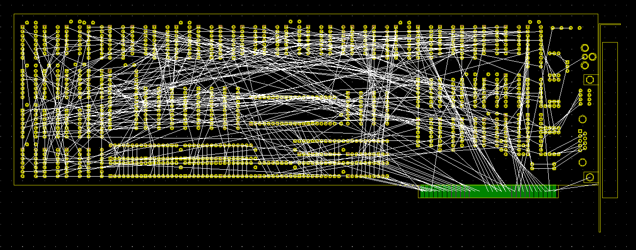
Note the many dozens of horizontally sloping lines; this is a clue that many trace runs will be necessary from one end of the board to the other. Given the lack of vertical room, its likely that a four-layer board will be needed.
The trace routing step took weeks of dedicated attention. I found the key was to make small and steady progress from one part of the board, fanning out as necessary. I chose the ISA connector as a logical place to start:
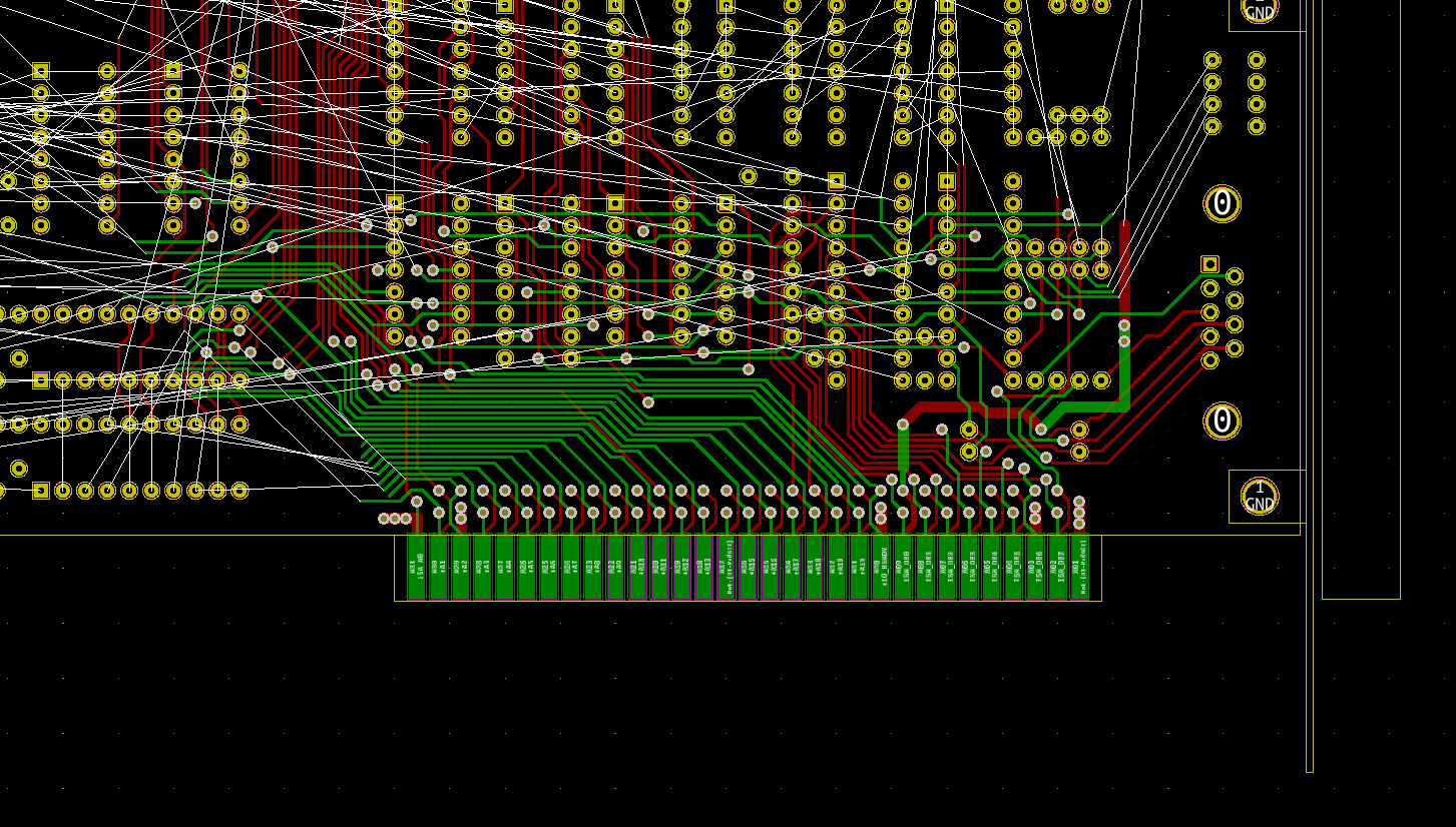
The air-net wires (white lines showing direct line to destination pads from closest trace) were an adequate guide to direct the placements. Top-side traces in green were generally kept horizontal, and back-side traces in red were generally kept vertical.
Very early on it became obvious that this board could not be routed with only two layers. A four-layer design was implemented in Kicad, with 5V power and ground reserved for those two layers, unless absolutely necessary to trace internally across the board. If internal tracing was required, it was done on the 5V layer.
Some 3D views of the progress with the routing around the ISA card edge connector:
A Significant Time Later:
It’s at this point that things really became a blur; I can’t overstate just how long this process took. A lot of trial-and-error was necessary in order to find workable routing solutions. This meant doubling back constantly, and adjusting on the fly as things didn’t work out. A lot of this work was conducted during a holiday break in December of 2019, when I had much more free time at hand, and many hours a day to throw at this.
The design evolved many times during this process, with additions or changes to the board in line with the initial “guiding principles” laid out in part one of this series of posts. Try as hard as I might, a fair number of the horizontal traces had to be routed internally on the 5V layer.
Rather than show each tedious step of this process, I’ll skip straight to the final design.
Final trace route:
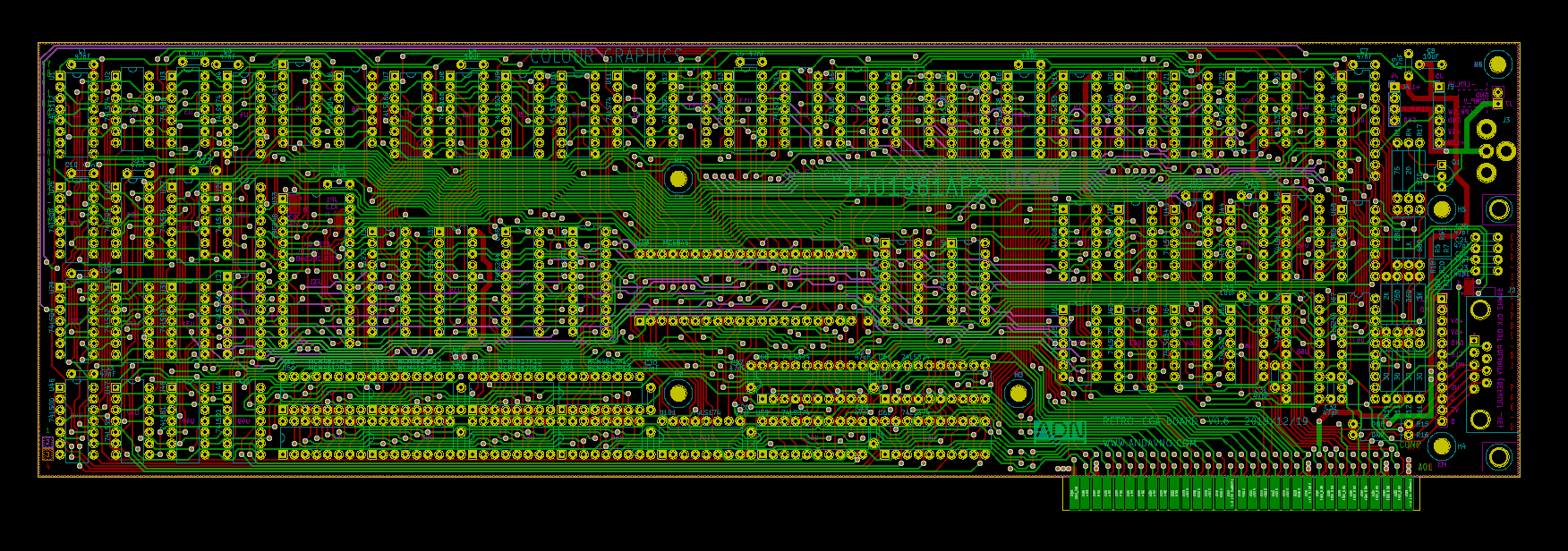
Zoomed-in view showing just how packed the horizontal tracing is around the video memory:

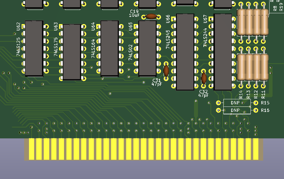
Top-side 3D view:

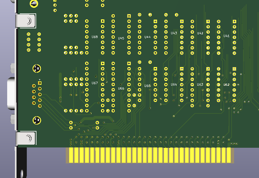
Bottom-side 3D view:

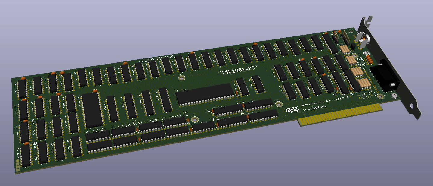
Isometric 3D view:
I’m very happy to have got to this stage, if only so that I can stop sinking time into it and get some sleep. But I jest, sleep will evade me.
Can’t Stop Now; More To Go:
So that’s quite a bit to digest, and the time period that I’m trying to capture in this single post spans several weeks, with a lot going on in those weeks.
Rather than lengthen this already long post, I’ll reserve a follow up to go over the various little details that made it into the design thus far. I’ll also cover some of the stumbling-blocks that I have thus far glossed over with respect to the schematic (some may already pick out what the issue is).
In the longer term, I’ll go on to describe the process of having these boards manufactured, assembling them, and testing them.
I hope that you the reader have enjoyed this project so far. Please join me again soon for another recap of the progress to date.