The last post in my series on retrocomputing covered the testing of my repaired CGA with the Micro 8088. The process of troubleshooting took several weeks, and it became apparent that a handy piece of hardware to have would be an ISA “POST Card“. This type of card is designed to display a series of diagnostic codes that are generated by the BIOS as it reaches certain milestones in its execution. This would have been very handy to have as a means of verifying if the Micro 8088 is functioning normally and executing BIOS code.
It is possible to buy an ISA POST card off eBay, but in the back of my mind I am wanting to learn how to use the KiCad software package to design and produce circuit boards. This may be the perfect excuse to design a POST card using KiCad, and do a whole lot of learning along the way.
Up to this point I had exclusively used Eagle 6.5.0 on a hobby license to design my circuit boards. This has been pretty limiting as the maximum board size is capped at 100 mm x 80 mm, and I was restricted to using only two board layers.
Following Eagle’s acquisition my Autodesk, I was not at all impressed with the move to an annoying subscription model and a cloud-based version of the software. KiCad has the potential to be a better-featured replacement to Eagle, and also a way of avoiding subscription services and nebulous cloud-based computing. Not my thing.
First Impressions
Dave at EEVblog has produced a great pair of videos (#253 and #254) in which he installs and reviews KiCad. I had more or less the same impressions when first running KiCad. Rather than repeat them all here, I’d encourage you to have a watch.
In terms of the most noticeable differences to Eagle PCB:
- The board and schematic are not linked in the same way that they are in Eagle; one can work on the schematic or board independently without being nagged about it (i.e. both windows do not need to be open at the same time). In KiCad, one must remember to update the board manually by “pulling” the details in from the schematic. As far as I can tell, the flow of information is always from schematic to board, not the other way around (no back-annotating?)
- Most operations in KiCad are performed by hovering the mouse where it is needed and then pressing a keyboard shortcut key to perform a function. This is opposed to Eagle where a very specific function is selected in the toolbar first, and then the mouse used to interact with the schematic/board features by clicking. (I think there were keyboard shortcuts in eagle but I never really used them).
- There is no real “project control” in KiCad; it is not possible to use “save as” on a project to save a copy of of the relevant files. It is likewise difficult to save legacy copies of schematic/board files in KiCad. This makes version control quite irritating. The changes made to a schematic or board in KiCad are more or less permanent once the files are saved. In Eagle, the implementation of the concept of a project made a lot more sense.
Quirks
Some other quirks that I have noticed in KiCad:
- Annoyingly, the keyboard shortcuts are not exactly the same between the schematic editor and the board editor (I.e. “TAB” key to push/pull nets in the schematic vs. “d” key to push/pull traces in the pcb).
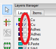
- The “active” layer is selected by clicking on, or to the left of, the little coloured squares that signify the different layer colours:

- The visibility of layers is controlled by clicking the check-boxes to the left of the layer names:
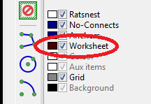
- There is an annoying maroon-coloured drawing frame visible in the background of the board editor. The relative location of this frame cannot be changed (to my knowledge anyway). It can be disabled by un-ticking the “Worksheet” layer on the “Items” tab of the layers manager:
- The design-rule-check process relies on “courtyards” which are defined in each footprint. If the “courtyard” areas of two components on the board overlap, then the DRC check will complain and throw an error. Annoyingly for some footprints, the courtyard areas are enormous and do not follow the physical limits of the component i.e. it is super easy to place them so that they overlap.
Starting the POST card
After getting used to the different UI style in KiCad, I shifted my attention to creating my first project. An ISA Post card.
It should come as no surprise that Sergey Kiselev has already created an ISA POST card that he has documented on the projects page of his website. I took a lot of inspiration from Sergey’s design, with some changes and additions to suit my whims.
Also of note: Sergey implemented a POST display function on his 16-bit ISA backplane (hosted on the RetroBrew Computers wiki). Some elements of this implementation were used for inspiration.
Another source of inspiration came from the following website. It shows a schematic and some details of 7-segment LED display addressing. I wish I knew the author’s full name; the only name I could find was “Bright”.
For my particular ISA POST card implementation, some of the “design whims” are:
- Ability to set the listening address with DIP switches.
- Using a type of very tiny 7-segment display “LTS-2801AG” which I have wanted to use for a while.
- Designed such that the 7-segment displays can be seen through the ISA card bracket (so that the POST codes can be read while the machine is assembled, for whatever use that may be).
Schematic
After getting used to it, the schematic creation in KiCad was honestly quite pleasant. The process of adding schematic symbols is quite easy and intuitive. The UI still catches me out sometimes: I kept forgetting that nets are “ended” away from pins by hovering the mouse and pressing the “k” key on the keyboard. Net nodes can be dragged by “hovering” the mouse over net vertices and pressing “g” on the keyboard. There is a lot less clicking than would be initially intuitive.
The finished schematic can be seen below:
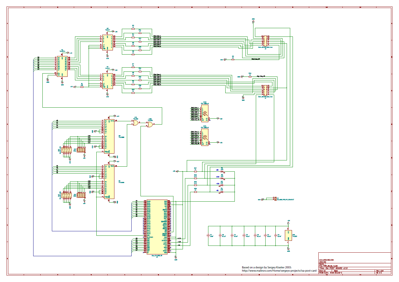
In the end, I implemented the variable addressing with 74LS688 chips and dip-switches (zoomed-in view on one bank of switches):
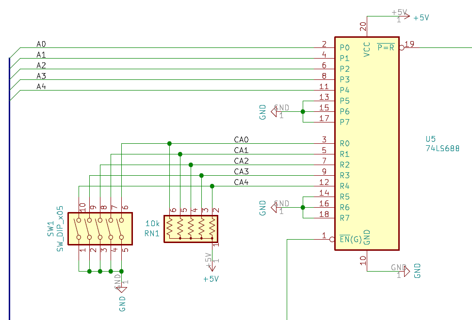
The schematic can be Downloaded Here (pdf file).
[Editor’s Note: Warning! Errors were discovered in this schematic. Can you spot them? Hint: look at the dip switch pull-up resistors and the logic gate circuitry employed via chip U2. It is unlikely this circuit would work as intended in its current state. It’s provided here for context to the rest of this article.]
ISA Card Dimensions
With the schematic completed, I move my attention to the board design. The card I intend to design is an 8-bit ISA card, obviously. But that begs the question: how on earth are ISA cards specified? What are the dimensional limits? This turns out to be a lot more confusing than one would think.
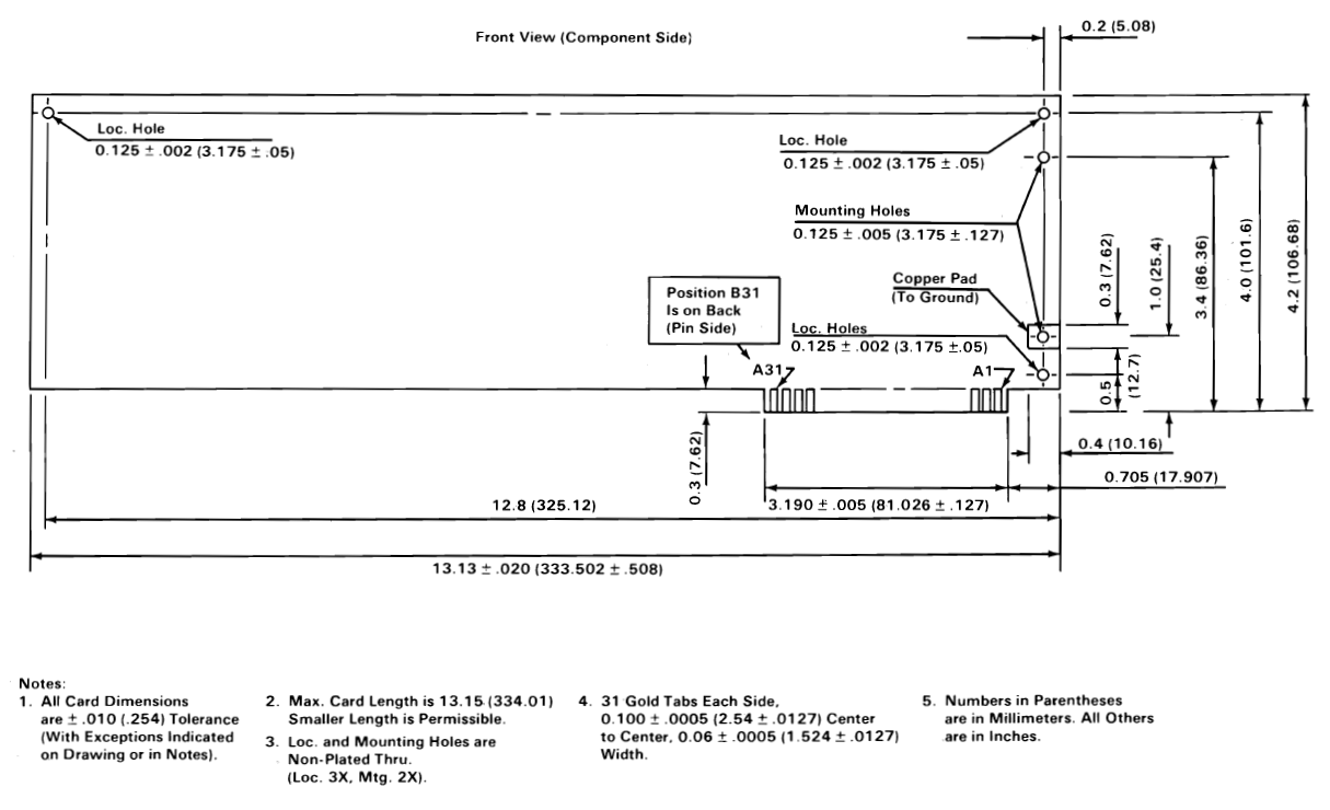
The bulk of the questions are answered by the IBM 5150 Technical Reference manual (IBM_5150_Technical_Reference_6322507_APR84.pdf). On page 54 of the pdf there is a super helpful diagram that explains the majority of the dimensions:
But wait! this is not the full story. The diagram shows a pair of mounting holes on the right hand side for some type of mounting bracket. Which bracket? Is the 0.705 inch overhang suited to this unknown type of bracket? How long can this overhang be if I want to use a different one? Is this distance referenced to the computer chassis somehow? Far too many questions left unanswered.
I’ll try to figure out the chassis reference first. The approach is to follow the dimension references down into the motherboard. To try and make this easy for myself, I’ll take the bottom centre of Pad A1 as the datum for the ISA card profile. I ended up finding some clues in the Intel ATX Specification. Relevant excerpt below (dimensions in inches):

So, the edge of the ATX motherboard would be the summation of 0.4 and 0.6 inches, which is 25.4 mm from Pin A1 of the ISA connector. Good start. Now how far is the motherboard from the chassis? The only info I could find was an article from a company called ProtoCase; an article called How to Design Custom Enclosures for Motherboard-Based Systems.
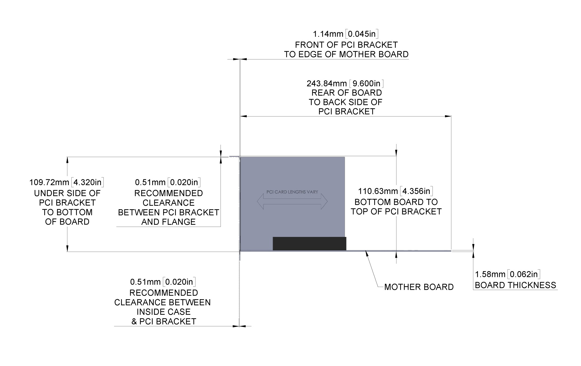
Figure 6-3 in the article explains that the distance from the front of the PCI bracket to the edge of the motherboard is 1.143 mm, and that there is a recommended clearance between the inside of the chassis and the front face of the PCI bracket of 0.508 mm.
So all in all, (if ProtoCase is to be believed) the face of the chassis would rest 27.051 mm from the centre-line of Pad A1 of the ISA card profile.
That’s the horizontal reference to the chassis sorted. What about vertical? the PC bracket gets screwed into a “shelf” on the chassis, but how far up is that from the ISA card edge connector?
A few different vendors sell an 8-bit ISA connector. I settled on a TE Connectivity part 6-5530843-5 (mouser), mostly because Sergey’s 8-bit Backplane happens to use it.
The datasheet for the ISA connector shows that the ISA card will “bottom out” at 0.315 inches (8.001 mm) from the top face of the motherboard:
 Jumping back to the ProtoCase reference dimensions: Figure 6-3 in the article gives a reference height from the underside of the motherboard to the underside of the ISA bracket of 109.728 mm. Again there is a recommended clearance between the chassis and the underside of the PCI bracket of 0.508 mm. lastly, there is a motherboard thickness of 1.58 mm.
Factoring all of those various reference heights; the height of the chassis “shelf” would rest 99.639 mm from the bottom-centre of Pad A1 of the ISA card profile.
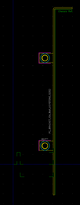
Now, The desired card bracket can be used to determine the appropriate hole locations in the ISA board profile (noting the recommended chassis clearance of 0.508 mm on the front face and underside of the bracket). In this instance, I am using a Keystone 9202 (mouser) card bracket.
For the sake of simplicity, I’ll leave out the derivations. The keystone mounting holes are located (20.3962 , 11.882) and (20.3962 , 68.397) in x,y coordinates from the bottom centre of Pad A1 of the card edge connector.
Frustrated by the lack of detail around ISA card specifications, I put together my own drawing, seen below:
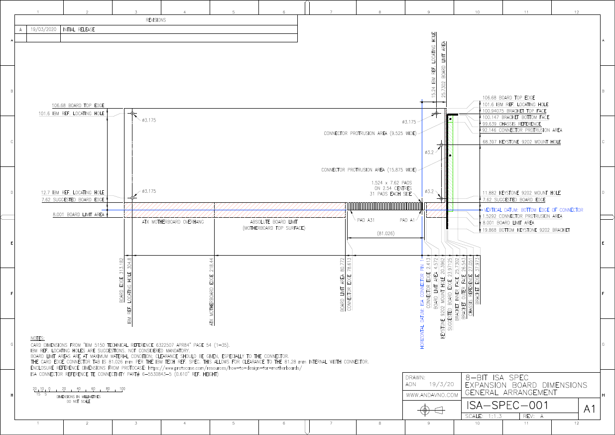
This drawing can also be Downloaded Here in pdf format for much better visibility.
Note the long list of caveats in the drawing notes; there are quite a few assumptions I am using to reach these dimensions.
Board Design
To be consistent with the board dimension findings above, I decided to create my own 8-bit ISA card edge footprint in KiCad. Note that the footprint origin is the bottom centre of Pad A01:

And again to be consistent, I decided to create my own Keystone 9202 bracket footprint. Note the footprint origin is the relative location of the bottom centre pad of A01:
The rest of the board buildup was relatively painless. One thing I enjoyed immensely was the “drag” function to move traces around the board and “nudge” them out of the way of one another. That’s a feature I’ve been sorely missing from Eagle while I still used it.
After many weeks of playing around with different layouts, I settled on the following:
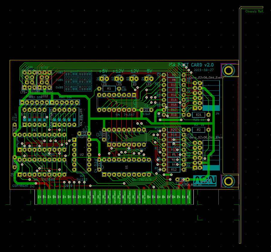
The cutout on the right hand side of the PCB (between the bracket mounting holes) is intended to house a small perpendicular daughterboard featuring 7-segment displays that can be seen through a cutout in the mounting bracket:

After I felt I had fussed over the design enough, I moved on to producing the Gerber files and sending the design files off for fabrication.
Ordering the Boards
I ordered the boards through Seeed Studio, and they arrived within a week or two:
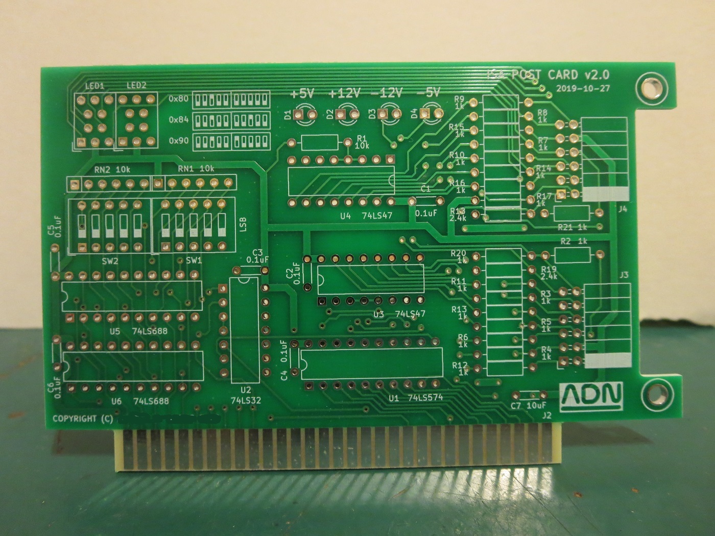
I was pretty happy with the finish (Hot air solder on pads, gold finish on fingers):
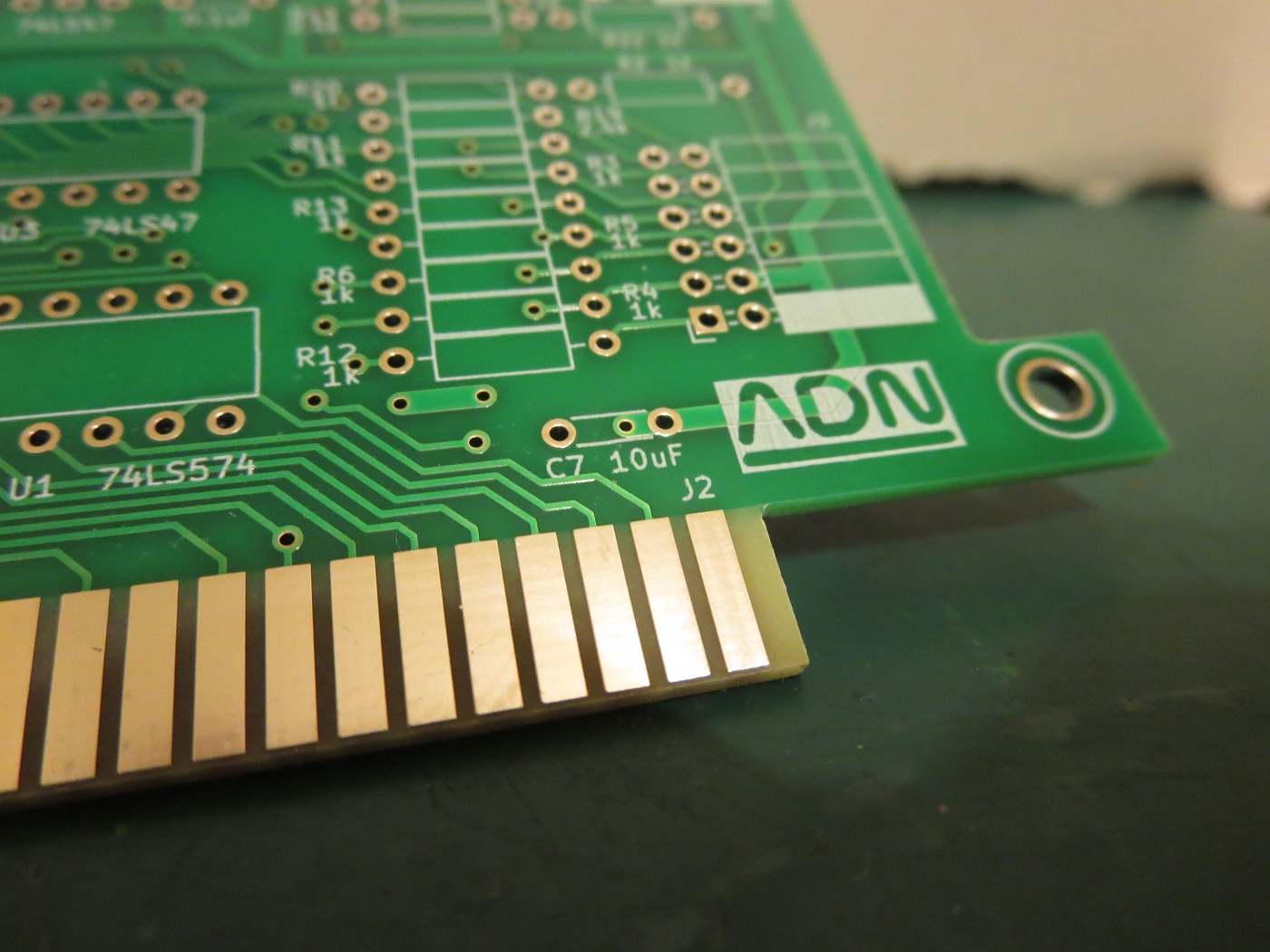 I set about soldering one of the boards together, but discovered a very silly mistake I made with one of the traces:

I had accidentally grounded the -5 volt rail by being careless with one of the traces and overlapping a ground pad on resistor R2. Ordinarily KiCad will not allow you to route a trace over a foreign pad, but It won’t protest if you move a footprint over a trace after it has been laid, which is what I must have done here. Another realisation: I did not do a Design Rules Check on the board before it was sent for fabrication. That would have certainly picked up this error before it got to this stage. Whoops. The fix was simple enough; cut the traces. By coincidence, the affected trace merely routes the -5 volt rail to be broken out on the adjacent pin header J3:
 With that hiccup out of the way, I completed the board:

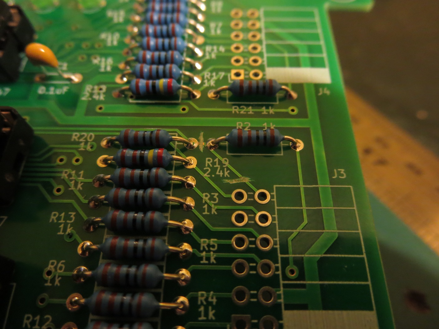
I picked up a second and third mistake in the process of testing the board.
The second mistake related to the DIP switches. I had not realised that I had wired them up the wrong way i.e. the associated pull-up resistors should have swapped 5v and ground:
This meant that the switches operate “backwards” to what is expected i.e. as the switch is moved upwards to the “on” position, it actually selects a logical bit “0” on the address bus. Whoops. I decided to leave this one alone for now as the fix would be too disruptive. I just need to remember that the switches work backwards.
The third mistake related to chip U2. I had accidentally messed up the gate logic linking the comparator chips U5 and U6 to the data latch chip U1. I had used a combination of OR-gates in a 74LS32 package, not realising that chip U5 and U6 outputs are active-low.
For a very sloppy fix I substituted a 74LS02 chip (NOR-gates) and reworked the circuit with magnet wire:
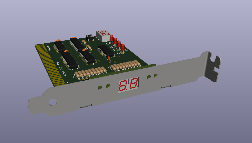
 After fixing the three mistakes, the board worked flawlessly in combination with Sergey’s Micro 8088 computer board and 8-bit ISA backplane:
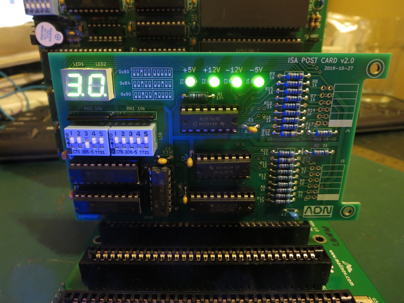
What a journey! I now have a functioning POST card that can be used to diagnose the state of the BIOS as it executes. This will come in very handy in the near future as I attempt to boot my retro-computer setup with my repaired CGA card.
At some point I will circle back and correct the silly mistakes on this POST card design. My intent will be to release it open-source when I am happy with it, and all the embarrassing mistakes are ironed out.
If you read this far, thank you! I appreciate the interest people may have in my hobby shenanigans and I hope it was informative, or at least somewhat entertaining.
Join my next retro-computing adventure as I try to boot the Micro 8088 into an operating system.
Very nice work! I loved to read it!
I’m also working on a private project – and searching all around the web the Keystone 9202 bracklet footprint and 3D model.
Would it be possible to share with the community? (in Grabcad.com and/or in Github in KiCAD library)
Thank you!
Hi Attila, please see my latest post “New Github”; I’ve added details of the Keystone 9202 to https://github.com/ausandavno/Kicad_Misc
Did you ever finalise your design?
Would love to build a POST card for my XT, based on your design.
Hi J, thank you for the interest! I have indeed finalised this design into a newer “v3” revision. The various bugs have been fixed, and I have added the ability to show HEX codes on the seven segment LEDs by mimicking a DM9368 chip with an ATF16V8B, as a sort-of-drop-in replacement to the 74LS47. I intend to release the v3 version on my GitHub page, along with the code for the ATF16V8B. This may be the push that I need to finally document the v3 design and the ATF16V8B code in new blog posts, and progress to loading on GitHub. I have been distracted with work as of late, but will aim to find the time in the coming weeks if able. -Andrew
Hi J, it’s taken me almost two years to finally progress the POST card design; please see my latest post https://www.andavno.com/?p=619. -Andrew
THANKS FOR YOUR LIBRARIES. YOU ARE THE ONLY ONE THAT MAKE LIBRARIES FOR ISA2.54MM
REGARDS FROM PUEBLA, MEXICO