The last post in this series showed some of the detail of the Retro-CGA as it has come together so far, and ended with the preparation of Gerber files in preparation of having some prototype boards fabricated.
After a week or two of waiting, the fabricated boards arrived in the mail. This post documents the assembly of one of the boards into a completed prototype.
The fabrication house that I used in the end was PCBWay. The Board Size was 337.82 x 106.68 mm, using four layers with mostly generic parameters (1.6mm thickness, 6/6mil track and space, min holes 0.3mm, gold fingers with 20 degree bevel, and ENIG finish over fingers and the rest of the board).
For a total quantity of five, the board cost was $177.00, the freight was $26.00, the “bank fee” was $10.00, and I used a $5.00 off coupon. Amounts in USD. Each of the five individual boards ended up costing $41.60 USD.
Pretty expensive in hindsight, but I think the four-layer nature of the board is driving up the cost considerably. On the other hand, not a bad price for something I couldn’t make myself.
The Boards:
I’m generally very impressed with the quality of the boards that I received. Some minor scratches here or there but nothing particularly bad.
An image of the top side of one of the boards using a flat-bed scanner:

And an image of the back side:

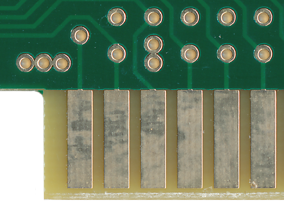
A closeup of the card edge connector shows a pretty good job with the bevelling of the lower edge:
 In the lower left hand corner of the top side of the card I’ve added some layer windows to try and see how good the alignment is. Layer two looks like it might be a few fractions of a millimetre out of alignment to the left:

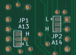
The silkscreen details look pretty good. This snapshot shows near the character ROM address jumpers on the back side of the card:
 Soldering:

Assembly was not too difficult, but quite tedious. I opted to use sockets for all of the ICs, and the only other large quantities of components were resistors and capacitors. There were 1,122 through hole pins to solder on the sockets alone. The entire process of soldering took approximately two hours.
To speed up the process of soldering the IC sockets, I firstly loaded them “dry” in position from the top side of the board. I then laid a flat piece of glass over all of the sockets, and inverted the board with the glass, making sure to hold the PCB firmly against the glass during the process.
By inverting the board and glass, the IC sockets end up upside down on top of the glass, with all of the leads poking upwards through the PCB, readily accessible for soldering. Glass was chosen to help keep the sockets nice and flat relative to one another.
After soldering over 1,250 pads, the prototype board began to take shape:

Buying Secondhand ICs:
The CRTC controller and the video RAM that featured on the original CGA are no longer manufactured. Early on in the process of designing the Retro-CGA, the choice was made to keep both of these chip types in the design in order mimic the behaviour as closely as possible. The end effect is to increase the difficulty in finding and purchasing these chips. Thankfully, these chips can still be sourced from second hand resell markets.
For the HD6845P CRTC controller, I ended up buying from Utsource. The exact listing is here. In case the listing expires, the chip was found by searching for “HD6845P” or “HD46505RP” and making sure the listing refers to a “DIP-40” chip package.
For the video DRAM, I ended up buying the “MB8118-12” from a website called Console5. The exact listing is here. I chose this chip because it was readily available and relatively cheap. Apparently the MB8118-12 is compatible with other 16Kb x 1 DRAMs like Intel 2118, Hitachi HM4816AP, Motorola MCM4517P, and Mostek MK4116.
The remainder of ICs (a whole load of logic chips and the character ROM chip) were sourced from Mouser.
The Completed Board:
After assembling the board and procuring the chips, the next step involved loading every IC into its corresponding socket! There are 69 socketed chips on this board, so this should be a fun exercise.
The tedious part of this process ended up being the folding of all the IC legs to fit in their sockets. Most DIP package ICs come with approximately 10 degrees of splay on the legs, so in order to fit within a socket they need to be gently bent ahead of time. There are tools that do this, but I don’t have any at hand. I ended up rocking them on their edges on an anti-static mat to slowly bend the legs into shape.
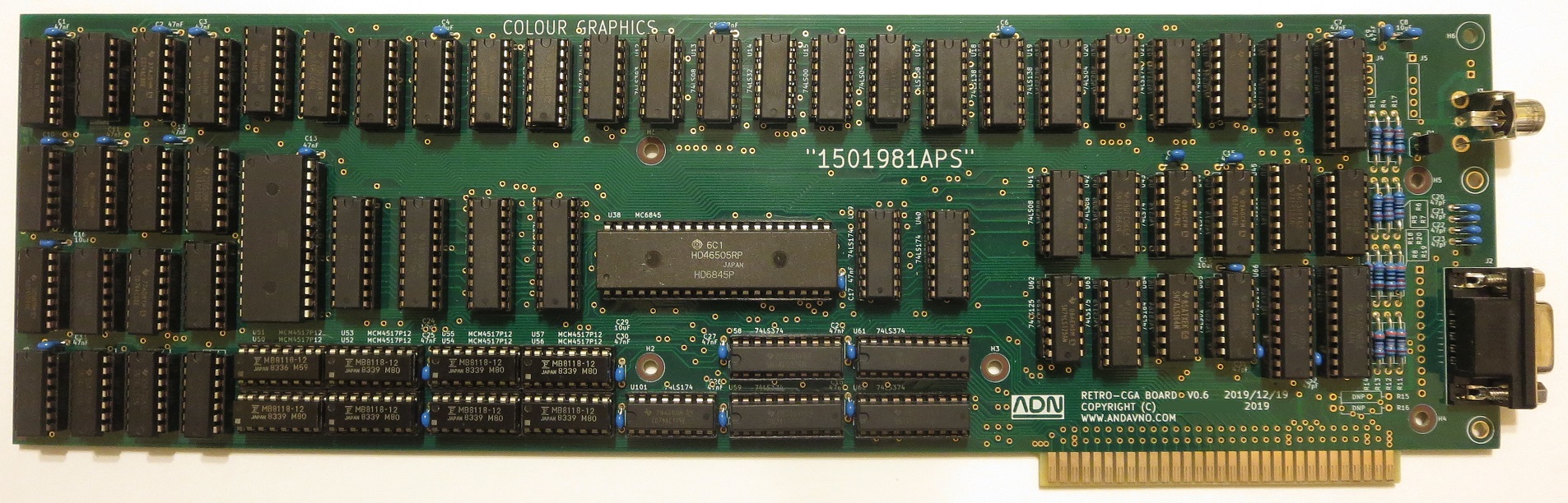
After loading all of the chips, the completed board emerges:
Hooray! I’m excited by this progress so far.
Next Steps:
One of the next steps will be to load the character ROM with the desired font, and then finally test the board with Sergey’s Micro 8088 computer board.
As always, I hope you have enjoyed this project so far. Please join me next time for the loading of the character ROM and the first test of this prototype board in an 8088 system.