In one of my last posts I pondered the journey required to create an open-source video card inspired by the CGA card that I had repaired, in an attempt to preserve its historically-significant legacy.
In this post I will share the progress I’ve made on undertaking that journey, using the various guiding principles discussed in the initial post.
In what I presume will take months of effort, let’s launch into the design of the “Retro-CGA”.
The first step in this process is the production of a schematic.
Searching for inspiration for the Retro-CGA design, I came across the schematics contained in the “IBM Color/Graphics Monitor Adapter” chapter of the IBM Personal Computer Hardware Reference Library. External link to pdf here (page 32 onward).
Although these schematics are a good starting point, I have no idea if they are accurate or relevant to the CGA design that would be representative of the card that I have repaired. It is likely that many aspects of these schematics will need to be adjusted to work with modern ICs, or to eliminate accidental mistakes that may have been introduced when they were first published.
I’ll continue using these schematics for inspiration, somewhat apprehensive in the knowledge that I’ll need to tackle any issues as they arise.
Schematic Build-up:
Following the design of a POST card, I’ve managed to get quite comfortable with the Kicad software package for schematic design and board generation. There are some things that I’m still getting used to, like proper library setup and library maintenance, but for the most part it has been a tolerable transition from Eagle PCB.
By using Kicad for the schematic and board design, I’ll be able to meet the long-term intent of releasing the Retro-CGA design as open-source.
Logic Gates:
Most 74-series logic chips are contained in the default Kicad library. Kicad deals with logic gates in a nifty way; each individual gate within an IC package can be placed as a stand-alone symbol. This makes schematic generation a lot easier; individual gates can be placed across many different schematic sheets, but still tied back to one discrete footprint.
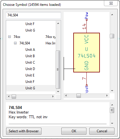
The way to do this is to begin by inserting a new symbol, typing the name of the intended chip (e.g. 74LS04), then expanding the menu tree to access the individual gates:

After the gate symbol is placed in the schematic, Kicad gives it a corresponding reference letter trailing the symbol Reference Field (the letter relates to the pin numbers used in the gate symbol):

All that is required to group gate symbols into one discrete package is to re-name them so that the Reference designation is consistent across them. E.g. renaming them all to “U2”.
There is one catch: you must also place in your schematic a symbol that describes the power pins of the discrete logic IC package (usually last in the list of choices):
As long as all of the individual gate (and power) symbols are named consistently, Kicad knows to tie them all to the one discrete logic IC. Very nice.
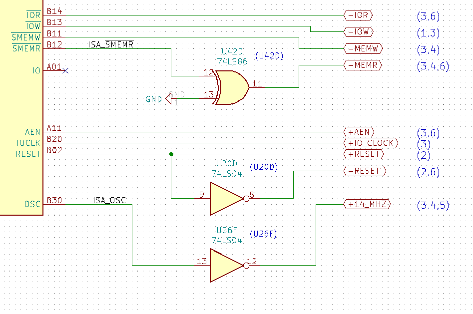
An example of using discrete logic gates in the Retro-CGA design:
Special Symbols:
As vast as the default symbol library is in Kicad, some components will be missing. This is usually the case for legacy components that have long since gone out of production. Fair enough, really.
In the case of the CGA, the symbols for the CRTC controller, the video memory and the character ROM are not contained in the default Kicad library. These components need to be replaced by modern equivalents and/or drawn by hand.
I won’t go in to too much detail of the process of creating a new symbol; there are many tutorials online showing how to do this. The Kicad process is quite intuitive and quick, and certainly different than Eagle. In Eagle, symbols and footprints were linked together by connecting pins and pads “by hand”, whereas Kicad relies on a consistent naming convention between symbols and footprints to make the connections automatically.
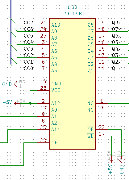
The CRTC Controller:
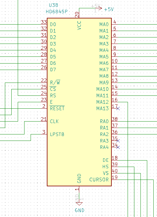
The most important chip on the original CGA video card was arguably the CRTC controller, which controls aspects of video timing and access to video memory. This chip appears as the big 40-pin DIP package near the centre of an original CGA card. There is no way to design-out this chip as there are no modern equivalents. Even if there was a modern equivalent, many of the behavioural quirks of the original IBM (colour palettes, text mode quirks, etc) are due to the presence of the particular controller chip that was used. The broad CRTC controller appears to be the 6845. Several variations of this chip exist, but one example appears to be the Hitachi HD6845P. Luckily these chips are still available in some limited quantities on second-hand IC resell markets such as Utsource. The Hitachi HD6845P appears to be obtainable on the resell markets, so this is the chip that will be used in the Retro-CGA design.
Creating the symbol for the HD6845P was relatively quick and easy:
The DRAM Video Memory:
The DRAM video memory on the original CGA is a little strange compared to nowadays; each chip is arranged as an array of 16,384 words of 1-bit in length. Eight individual memory chips are used in parallel to achieve 1 byte of storage per each of the 16,384 words in address space.
Another oddity; there are only 7 pins available to interface to the address space in the chip. The full 14-bit address space is accessed by writing two sequential 7-bit address halves into the chip and strategically toggling the CAS (column address strobe) and RAS (row address strobe) pins on the chip.
There appear to be many different variants of this type of chip available over the years: Intel 2118, Hitachi HM4816AP, Motorola MCM4517P, Mostek MK4116, Fujitsu MB8118.
In terms of the CGA design, this particular type of chip would have no direct modern equivalent. Thankfully, DRAM chips of this type are still available through second-hand resell markets.
The DRAM would be a good contender for switching to a modern equivalent, but the CAS and RAS circuitry appears to be linked in to other parts of the circuit and may be difficult to modify without breaking the inherent nature of the HD6845P. For now at least, I will keep the legacy part for the DRAM.
For the purposes of creating a symbol, I chose the Motorola MCM4517P, but any generic memory chip of the same type/family should be equivalent.
The Motorola MCM4517P as drawn as a brand new symbol:

The Character ROM:
The last special chip is the character ROM. This is the large-ish chip to the left-hand side of the 40-pin CRTC controller chip on the original CGA. This chip is typically labelled “MK36906N-4”. This is a 64k-bit read only memory manufactured by Mostek under the “MK36000” series of memory ICs. Unfortunately, each of these chips would have been factory programmed with the contents of the character ROM, and none would have been commercially available back in the day, let alone today.
A close equivalent for this chip is apparently the 27C64 series of EPROM, but this type of chip does not appear to be commercially produced. The 27C64 may be available on the second-hand resell market, but they may be difficult to program without a particular type of programmer.
The next closest equivalent appears to be the AT28C64 which is an EEPROM. Thankfully, this chip is still commercially produced, with only minor differences to the 27C64. This should do for the purposes of a character ROM replacement.
The AT28C64 as drawn as a brand new symbol:
Schematic Oddities:
Some parts of the schematic in the “IBM Color/Graphics Monitor Adapter” chapter of the IBM Personal Computer Hardware Reference Library are difficult to understand.
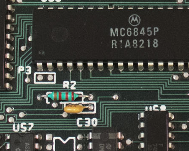
Weird ROM pull-up resistor:
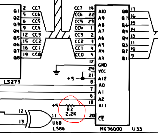
Resistor R2 doesn’t appear to do anything. For comparison, pin A12 of the ROM is pulled high to 5v without any resistor. So why is this one necessary? From background research, this appears to be a legacy detail from an early revision of the CGA card in which the “thin font” style could be selected by jumper P3, close to the CRTC controller:
It seems like later revisions of the CGA retained resistor R2, but not the P3 header. It is probable that the P3 header would short the A11 pin of the ROM to ground, enabling the use of the “thin font” characters contained in the lower address space of the ROM. This detail was discarded for the Retro-CGA design (i.e. resistor R2 removed).
A signal is broken out of the the video DRAM address bus in a confusing way:
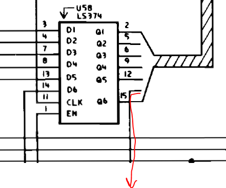
This was quite irritating to try and parse, at least in my mind. What part of the address bus does the red signal trace relate to? Is it pin 15 of U58? If that’s the case, what pin is Q6 supposed to be?
After a lot of head scratching, I believe the trace is supposed to be address bus bit “A5”, with the equivalent circuit as:
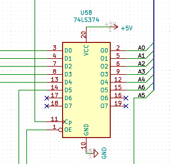
With the “O6” and “O7” outputs of the U58 not connected. I hope this interpretation is correct.
Unnamed buffer gate adjacent to R18:

By deduction and proximity, this gate belongs to U67, which is buffering the signals out of the RGBI connector on the card. It seems like the remainder of the available gates of U67 were used to buffer the Blue and Red signals into the composite video output circuitry, but that particular gate was left out of the dotted bounding box of U67 for whatever reason.
The remainder of the annotation of the schematic proceeded with relatively minor issues. When a logic chip was not contained in the default Kicad library, it was drawn by hand.
Completed Schematics:
After weeks of effort, the schematics were completed to a somewhat competent degree. Enough to begin the board design at least. A poor-quality example of sheet number one is shown below:

I won’t be releasing the schematics or board files until I’ve undertaken rigorous troubleshooting of the design.
Hopefully you’ve enjoyed reading about this first step in the journey towards the Retro-CGA card. The next instalment of this series will focus on aspects of the board design.